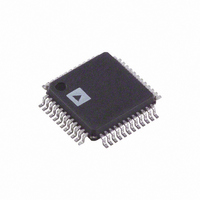
AD9244BST-40 Analog Devices Inc, AD9244BST-40 Datasheet - Page 3

AD9244BST-40
Manufacturer Part Number
AD9244BST-40
Description
IC ADC 14BIT 40MSPS 48-LQFP
Manufacturer
Analog Devices Inc
Datasheet
1.AD9244BSTZ-65.pdf
(36 pages)
Specifications of AD9244BST-40
Rohs Status
RoHS non-compliant
Number Of Bits
14
Sampling Rate (per Second)
40M
Data Interface
Parallel
Number Of Converters
1
Power Dissipation (max)
300mW
Voltage Supply Source
Analog and Digital
Operating Temperature
-40°C ~ 85°C
Mounting Type
Surface Mount
Package / Case
48-LQFP
For Use With
AD9244-65PCBZ - BOARD EVAL FOR AD9244-65AD9244-40PCBZ - BOARD EVAL FOR AD9244-40
Available stocks
Company
Part Number
Manufacturer
Quantity
Price
Company:
Part Number:
AD9244BST-40
Manufacturer:
ADI
Quantity:
210
Part Number:
AD9244BST-40
Manufacturer:
ADI/亚德诺
Quantity:
20 000
SPECIFICATIONS
DC SPECIFICATIONS
AVDD = 5 V, DRVDD = 3 V, f
differential analog inputs, unless otherwise noted.
Table 1.
Parameter
RESOLUTION
DC ACCURACY
TEMPERATURE DRIFT
INTERNAL VOLTAGE REFERENCE
INPUT REFERRED NOISE
ANALOG INPUT
POWER SUPPLIES
POWER CONSUMPTION
1
2
3
4
5
6
Gain error is based on the ADC only (with a fixed 2.0 V external reference).
Measured at maximum clock rate, f
Includes internal voltage reference error.
Input capacitance refers to the effective capacitance between one differential input pin and AGND. Refer to Figure 7 for the equivalent analog input structure.
Input bias current is due to the input looking like a resistor that is dependent on the clock rate.
Measured with dc input at maximum clock rate.
No Missing Codes
Offset Error
Gain Error
Differential Nonlinearity (DNL)
Integral Nonlinearity (INL)
Offset Error
Gain Error (EXT VREF)
Gain Error (INT VREF)
Output Voltage Error (2 VREF)
Load Regulation @ 1 mA
Output Voltage Error (1 VREF)
Load Regulation @ 0.5 mA
Input Resistance
VREF = 2 V
VREF = 1 V
Input Voltage Range (Differential)
Common-Mode Voltage
Input Capacitance
Input Bias Current
Analog Bandwidth (Full Power)
Supply Voltages
Supply Current
DC Input
Sine Wave Input
VREF = 2 V
VREF = 1 V
AVDD
DRVDD
IAVDD
IDRVDD
PSRR
6
1
5
4
3
1
2
IN
SAMPLE
2
= 2.4 MHz, full-scale sine wave, with approximately 5 pF loading on each output bit.
= 65 MSPS (–65) or 40 MSPS (–40), differential clock inputs, VREF = 2 V, external reference,
Temp
Full
Full
Full
25°C
Full
Full
Full
Full
25°C
25°C
25°C
25°C
Full
Full
Full
Full
Full
Full
Full
Full
Full
Full
Full
Full
Full
Full
25°C
Full
Full
Full
Full
Test
Level
VI
VI
VI
VI
VI
V
V
VI
V
V
V
VI
V
IV
V
V
V
V
V
V
V
V
V
V
IV
IV
V
V
V
V
VI
Min
14
−4
0.5
4.75
2.7
Rev. C | Page 3 of 36
AD9244BST-65
Typ
Guaranteed
±0.3
±0.6
±0.7
±1.4
±2.0
±2.3
±25
0.5
0.25
5
0.8
1.5
2
1
10
500
750
5
109
12
±0.05
550
590
Max
±1.4
±2.0
±1.0
+4
4
5.25
5.25
±29
±15
640
Min
14
−4
0.5
4.75
2.7
AD9244BST-40
Typ
Guaranteed
±0.3
±0.6
±0.6
±1.3
±2.0
±2.3
±25
0.5
0.25
5
0.8
1.5
2
1
10
500
750
5
64
8
±0.05
300
345
Max
±1.4
±2.0
±1.0
+4
±29
±15
4
5.25
5.25
370
AD9244
% FSR
% FSR
LSB
LSB
ppm/°C
mV
mV
% FSR
mW
Unit
Bits
Bits
LSB
LSB
ppm/°C
ppm/°C
mV
mV
kΩ
LSB rms
LSB rms
V p-p
V p-p
V
pF
μA
MHz
V
V
mA
mA
mW


