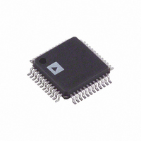
AD9244BST-40 Analog Devices Inc, AD9244BST-40 Datasheet - Page 23

AD9244BST-40
Manufacturer Part Number
AD9244BST-40
Description
IC ADC 14BIT 40MSPS 48-LQFP
Manufacturer
Analog Devices Inc
Datasheet
1.AD9244BSTZ-65.pdf
(36 pages)
Specifications of AD9244BST-40
Rohs Status
RoHS non-compliant
Number Of Bits
14
Sampling Rate (per Second)
40M
Data Interface
Parallel
Number Of Converters
1
Power Dissipation (max)
300mW
Voltage Supply Source
Analog and Digital
Operating Temperature
-40°C ~ 85°C
Mounting Type
Surface Mount
Package / Case
48-LQFP
For Use With
AD9244-65PCBZ - BOARD EVAL FOR AD9244-65AD9244-40PCBZ - BOARD EVAL FOR AD9244-40
Available stocks
Company
Part Number
Manufacturer
Quantity
Price
Company:
Part Number:
AD9244BST-40
Manufacturer:
ADI
Quantity:
210
Part Number:
AD9244BST-40
Manufacturer:
ADI/亚德诺
Quantity:
20 000
Clock Input Modes
Figure 55 to Figure 59 illustrate the modes of operation of the
clock receiver. Figure 55 shows a differential clock directly
coupled to CLK+ and CLK–. In this mode, the common mode
of the CLK+ and CLK– signals should be close to 1.6 V. Figure 56
illustrates a single-ended clock input. The capacitor decouples
the internal bias voltage on the CLK– pin (about 1.6 V), estab-
lishing a threshold for the CLK+ pin. Figure 57 provides
backward compatibility with the AD9226. In this mode, CLK−
is grounded, and the threshold for CLK+ is 1.5 V. Figure 58
shows a differential clock ac-coupled by connecting through
two capacitors. AC coupling a single-ended clock can also be
accomplished using the circuit in Figure 59.
When using the differential clock circuits of Figure 55 or Figure 58,
if CLK− drops below 250 mV, the mode of the clock receiver
may change, causing conversion errors. It is essential that CLK−
remains above 250 mV when the clock is ac-coupled or dc-coupled.
Clock Input Considerations
The analog input is sampled on the rising edge of the clock.
Timing variations, or jitter, on this edge causes the sampled
input voltage to be in error by an amount proportional to the
slew rate of the input signal and to the amount of the timing
variation. Thus, to maintain the excellent high frequency SFDR
and SNR characteristics of the AD9244, it is essential that the
clock edge be kept as clean as possible.
The clock should be treated like an analog signal. Clock drivers
should not share supplies with digital logic or noisy circuits.
The clock traces should not run parallel to noisy traces. Using a
pair of symmetrically routed, differential clock signals can help
to provide immunity from common-mode noise coupled from
the environment.
The clock receiver functions like a differential comparator. At
the CLK inputs, a slowly changing clock signal results in more
jitter than a rapidly changing one. Driving the clock with a low
amplitude sine wave input is not recommended. Running a high
speed clock through a divider circuit provides a fast rise/fall
time, resulting in the lowest jitter in most systems.
Figure 55. Differential Clock Input, DC-Coupled
CLK+
CLK–
AD9244
Rev. C | Page 23 of 36
Clock Power Dissipation
Most of the power dissipated by the AD9244 is from the analog
power supplies. However, lower clock speeds reduce digital
supply current. Figure 60 shows the relationship between power
and clock rate.
Figure 57. Single-Ended Input, Retains Pin Compatibility with AD9226
600
550
500
450
400
350
300
250
200
0
Figure 56. Single-Ended Clock Input, DC-Coupled
Figure 59. Single-Ended Clock Input, AC-Coupled
Figure 60. Power Consumption vs. Sample Rate
Figure 58. Differential Clock Input, AC-Coupled
10
AGND
AGND
AGND
TO 0.1μF
20
100pF
0.1μF
0.1μF
0.1μF
1.6V
1.6V
SAMPLE RATE (MHz)
30
CLK+
CLK–
CLK+
CLK–
CLK+
CLK–
AD9244-40
CLK+
CLK–
40
AD9244
AD9244
AD9244
AD9244
50
AD9244-65
60
AD9244
70


