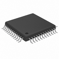
MAX1197ECM+TD Maxim Integrated Products, MAX1197ECM+TD Datasheet - Page 5

MAX1197ECM+TD
Manufacturer Part Number
MAX1197ECM+TD
Description
IC ADC 8BIT 60MSPS DL 48-TQFP
Manufacturer
Maxim Integrated Products
Datasheet
1.MAX1197ECMD.pdf
(22 pages)
Specifications of MAX1197ECM+TD
Number Of Bits
8
Sampling Rate (per Second)
60M
Data Interface
Parallel
Number Of Converters
2
Power Dissipation (max)
150mW
Voltage Supply Source
Single Supply
Operating Temperature
-40°C ~ 85°C
Mounting Type
Surface Mount
Package / Case
48-TQFP Exposed Pad, 48-eTQFP, 48-HTQFP, 48-VQFP
Lead Free Status / RoHS Status
Lead free / RoHS Compliant
ELECTRICAL CHARACTERISTICS (continued)
(V
resistor, V
noted. ≥ +25°C guaranteed by production test, < +25°C guaranteed by design and characterization. Typical values are at T
Input Low Threshold
Input Hysteresis
Input Leakage
Input Capacitance
DIGITAL OUTPUTS (D7A–D0A, D7B–D0B)
Output Voltage Low
Output Voltage High
Three-State Leakage Current
Three-State Output Capacitance
POWER REQUIREMENTS
Analog Supply Voltage Range
Output Supply Voltage Range
Analog Supply Current
Output Supply Current
Analog Power Dissipation
Power-Supply
Rejection
TIMING CHARACTERISTICS
CLK Rise to Output Data Valid
Time
OE Fall to Output Enable Time
OE Rise to Output Disable Time
CLK Pulse Width High
CLK Pulse Width Low
DD
= OV
Dual, 8-Bit, 60Msps, 3V, Low-Power ADC with
IN
DD
PARAMETER
= 2V
= 3V, 0.1µF and 2.2µF capacitors from REFP, REFN, and COM to GND; REFOUT connected to REFIN through a 10kΩ
P-P
(differential with respect to COM), C
_______________________________________________________________________________________
Internal Reference and Parallel Outputs
SYMBOL
t
t
DISABLE
ENABLE
V
PDISS
OV
I
C
PSRR
I
OVDD
V
I
LEAK
V
V
HYST
C
t
t
VDD
t
V
I
I
OUT
DO
CH
CL
OH
DD
IH
OL
IL
IL
IN
DD
CLK
PD, OE, SLEEP, T/B
V
V
I
I
OE = OV
OE = OV
C
Operating, f
-1dB FS applied to both channels
Sleep mode
Shutdown, clock idle, PD = OE = OV
Operating, f
-1dB FS applied to both channels (Note 6)
Sleep mode
Shutdown, clock idle, PD = OE = OV
Operating, f
-1dB FS applied to both channels
Sleep mode
Shutdown, clock idle, PD = OE = OV
Offset, V
Gain, V
C
Clock period: 16.67ns (Note 7)
Clock period: 16.67ns (Note 7)
SINK
SOURCE
IH
IL
L
L
= 15pF
= 20pF (Notes 1, 7)
= 0
= V
L
= -200µA
= 10pF at digital outputs, f
DD
DD
DD
DD
DD
= 200µA
= OV
±5%
INA & B
INA & B
INA & B
±5%
CONDITIONS
DD
= 20MHz at
= 20MHz at
= 20MHz at
CLK
DD
DD
DD
= 60MHz, T
OV
- 0.2
MIN
2.7
1.7
A
DD
= T
MIN
8.33 ± 1.5
8.33 ± 1.5
T YP
0.15
120
to T
0.1
0.3
40
±3
±3
5
5
3
3
3
9
3
3
9
6
5
5
MAX
, unless otherwise
OV
MAX
0.2 ×
0.2 ×
V
±20
±20
±10
150
0.2
3.6
3.6
50
20
10
60
DD
9
DD
A
= +25°C.)
UNITS
mV/V
mW
mA
mA
µW
µA
pF
µA
pF
µA
µA
ns
ns
ns
ns
ns
V
V
V
V
V
V
5


