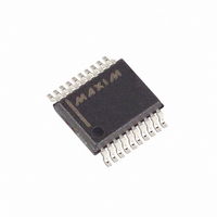
MAX152CAP+ Maxim Integrated Products, MAX152CAP+ Datasheet - Page 2

MAX152CAP+
Manufacturer Part Number
MAX152CAP+
Description
IC ADC 8BIT 1UA PWR-DWN 20-SSOP
Manufacturer
Maxim Integrated Products
Datasheet
1.MAX152CWP.pdf
(12 pages)
Specifications of MAX152CAP+
Number Of Bits
8
Sampling Rate (per Second)
400k
Data Interface
Parallel
Number Of Converters
3
Power Dissipation (max)
640mW
Voltage Supply Source
Dual ±
Operating Temperature
0°C ~ 70°C
Mounting Type
Surface Mount
Package / Case
20-SSOP
Lead Free Status / RoHS Status
Lead free / RoHS Compliant
+3V, 8-Bit ADC with 1µA Power-Down
V DD to GND .............................................................-0.3V to +7V
V SS to GND ..............................................................+0.3V to -7V
Digital Input Voltage to GND ........................-0.3V, (V DD + 0.3V)
Digital Output Voltage to GND .....................-0.3V, (V DD + 0.3V)
VREF+ to GND................................(V SS - 0.3V) to (V DD + 0.3V)
VREF- to GND.................................(V SS - 0.3V) to (V DD + 0.3V)
V IN to GND .....................................(V SS - 0.3V) to (V DD + 0.3V)
ELECTRICAL CHARACTERISTICS
(Unipolar input range, V
mode (pin 7 = GND), T
ABSOLUTE MAXIMUM RATINGS
Stresses beyond those listed under “Absolute Maximum Ratings” may cause permanent damage to the device. These are stress ratings only, and functional
operation of the device at these or any other conditions beyond those indicated in the operational sections of the specifications is not implied. Exposure to
absolute maximum rating conditions for extended periods may affect device reliability.
2
ACCURACY (Note 1)
Resolution
Total Unadjusted Error
Differential Nonlinearity
Zero-Code Error (Note 2)
Full-Scale Error (Note 2)
DYNAMIC PERFORMANCE (Note 3)
Signal-to-Noise Plus
Distortion Ratio
Total Harmonic Distortion
Spurious-Free Dynamic Range
Input Full-Power Bandwidth
Maximum Input Slew Rate, Tracking
ANALOG INPUT
Input Voltage Range
Input Leakage Current
Input Capacitance
REFERENCE INPUT
Reference Resistance
VREF+ Input Voltage Range
VREF- Input Voltage Range
_______________________________________________________________________________________
PARAMETER
A
DD
= T
= 3.0V to 3.6V, GND = 0V, V
MIN
to T
MAX
, unless otherwise noted.)
SYMBOL
S/(N+D)
RREF
TUE
DNL
THD
C
V
N
I
IN
IN
IN
SS
Unipolar range
No-missing-codes guaranteed
Unipolar and bipolar modes
Unipolar and bipolar modes
MAX152C/E, f
400kHz, f
MAX152M, f
f
MAX152C/E, f
400kHz, f
MAX152M, f
f
MAX152C/E, f
400kHz, f
MAX152M, f
f
V
V
IN
IN
IN
IN
SS
= GND, VREF+ = 3.0V, VREF- = GND, specifications are given for RD
= 30.725kHz
= 30.725kHz
= 30.725kHz
= 3.0V
< V
CONDITIONS
IN
IN
IN
IN
< V
p-p
= 30.273kHz
= 30.273kHz
= 30.273kHz
SAMPLE
SAMPLE
SAMPLE
Continuous Power Dissipation (T A = +70°C)
Operating Temperature Ranges:
Storage Temperature Range .............................-65°C to +150°C
Lead Temperature (soldering, 10sec) .............................+300°C
DD
SAMPLE
SAMPLE
SAMPLE
Plastic DIP (derate 11.11mW/°C above +70°C) ..........889mW
Wide SO (derate 10.00mW/°C above +70°C)..............800mW
SSOP (derate 8.00mW/°C above +70°C) ....................640mW
CERDIP (derate 11.11mW/°C above +70°C) ...............889mW
MAX152C__ ........................................................0°C to +70°C
MAX152E__ .....................................................-40°C to +85°C
MAX152MJP ..................................................-55°C to +125°C
= 340kHz,
= 340kHz,
= 340kHz,
=
=
=
VREF-
VREF-
0.28
MIN
V
45
45
50
50
8
1
SS
TYP
0.3
0.5
22
2
MAX
VREF+
VREF+
V
-50
-50
±1
±1
±1
±1
±3
4
DD
UNITS
MHz
V/µs
LSB
LSB
LSB
LSB
Bits
dB
dB
dB
µA
pF
kΩ
V
V
V


