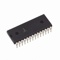
HI3-7159A-5 Intersil, HI3-7159A-5 Datasheet - Page 2

HI3-7159A-5
Manufacturer Part Number
HI3-7159A-5
Description
CONV A/D 5.5 DIGITIC MPU 28-DIP
Manufacturer
Intersil
Datasheet
1.HI3-7159A-5.pdf
(14 pages)
Specifications of HI3-7159A-5
Number Of Bits
8
Sampling Rate (per Second)
200k
Data Interface
Serial, Parallel
Number Of Converters
1
Voltage Supply Source
Analog and Digital, Dual ±
Operating Temperature
0°C ~ 70°C
Mounting Type
Through Hole
Package / Case
28-DIP (0.600", 15.24mm)
Lead Free Status / RoHS Status
Contains lead / RoHS non-compliant
Available stocks
Company
Part Number
Manufacturer
Quantity
Price
Absolute Maximum Ratings
Supply Voltage
Digital Pins, (pins 15 - 28) . . . . . . . . D
Analog Pins, (pins 2 - 13). . . . . . . . . . .V
Operating Conditions
Temperature Range . . . . . . . . . . . . . . . . . . . . . . . . . . . 0
CAUTION: Stresses above those listed in “Absolute Maximum Ratings” may cause permanent damage to the device. This is a stress only rating and operation of the
device at these or any other conditions above those indicated in the operational sections of this specification is not implied.
NOTE:
Electrical Specifications
NOTES:
Integral Non-Linearity, INL
Ratiometric Reading
Zero Error, ZE
Voltage Range of V
(Pin 13), V
Voltage Range of V
(Pin 12), V
Common Mode Rejection, CMR
Input Leakage Current, I
Input Capacitance, C
Noise (Peak-to-Peak Value, Not
Exceeded 95% of Time), e
Zero Drift, T
Full Scale Error Tempco, T
Supply Range, V
V
V
Digital GND Current, I
Analog GND Current, I
V
PSR
Guard Driver Pins 5, 8
Output Current, I
1.
2. All typical values have been characterized but are not production tested.
3. Not production tested, guaranteed by design and characterization.
4. Reference adjusted for correct full-scale reading.
5. V
V
V
CC
EE
CC
CC
EE
V
V
JA
, V
Supply Current, I
IN
CC
EE
Supply Current, I
to GND (A
to GND (A
EE
is measured with the component mounted on an evaluation PC board in free air.
= V
IN LO
IN HI
Power Supply Rejection,
IN HI
C(ZE)
PARAMETER
- V
GND
GND
OGD
SUPPLY
IN LO
IN LO
IN HI
/D
IN
/D
EE
CC
DGND
AGND
GND
GND
IN
.
Input
Input
N
C(FSE)
) . . . . . . . . . . . . . . +0.3V < V
) . . . . . . . . . . . . . . -0.3V < V
2
Test Conditions: V
f
Compensated Mode, Unless Otherwise Specified
CLOCK
GND
EE
-2V to 0V (Notes 2, 3, 4, 5)
V
V
-2V
-2V
V
Pins 9, 10, 12, 13, V
Pins 9, 10, 12, 13
V
V
V
V
V
0V to +2V (Notes 2, 3, 4, 5)
IN HI
IN HI
IN HI
IN HI
IN HI
IN HI
EE
IN
-0.3V < V
-0.3V < V
= 2.40MHz, R
(Pins 9, 10) = +3V, -3V
= -4.75V to V
V
V
= V
= 0.00000V
= V
= 0.00000V
= 2.00000V
= V
IN HI
IN HI
REF HI
IN LO
REF HI
A
D
CC
TEST CONDITIONS
- V
- V
< V
<V
o
= +5V, V
INT
IN LO
IN LO
C to 70
= -3V to +3V
CC
CC
CC
CC
= 1.00000V
= 1.00000V, V
CC
= 400k , C
< +6V
+0.3V
+0.3V
IN
< -6V
= +5.50V, V
= +3V, -3V
o
2V
2V
HI-7159A
EE
C
= -5V, D
INT
CC
EE
= 0.01 F, T
GND
= +4.75V,
Thermal Information
Thermal Resistance (Typical, Note 1)
Maximum Junction Temperature . . . . . . . . . . . . . . . . . . . . . . 150
Maximum Storage Temperature, T
Maximum Lead Temperature (Soldering 10s) . . . . . . . . . . . . 300
= -5.50V
PDIP Package . . . . . . . . . . . . . . . . . . . . . . . . . . . . .
= 0V, A
A
GND
= 25
V
IN LO
99996
+4.75
-4.75
o
MIN
= 0V, V
C, V
-1
10
-
-
-
-
-
-
-
-
-
-
-
-
-
-
-2V
IN LO
REF HI
= A
100000
0.0015
0.0015
TYP
+5.0
GND
-5.0
= +1.00000V, V
+3
0.1
0
3
5
0
3
-
-
-
-
-
-
-
1
STG
, C
REF
. . . . . . . . . . -65
V
= 1.0 F, 5
IN LO
100003
0.0035
0.0035
MAX
+5.5
-5.5
4.5
5.5
10
REF LO
0.1
1
-
-
-
-
-
-
-
-
1
+2V
1
/
= AGND,
2
Digit
o
Counts/
Counts/
C to 150
Counts
Counts
Counts
Counts
Counts
UNITS
JA
% FS
% FS
mA
mA
mA
pF
V
V
V
V
(
50
A
A
A
o
C/W)
o
o
C
C
o
o
o
C
C
C


