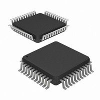
HI5762/6IN Intersil, HI5762/6IN Datasheet - Page 11

HI5762/6IN
Manufacturer Part Number
HI5762/6IN
Description
CONV A/DDUAL 10BIT 60MSPS 44MQFP
Manufacturer
Intersil
Datasheet
1.HI57626IN.pdf
(16 pages)
Specifications of HI5762/6IN
Number Of Bits
10
Sampling Rate (per Second)
60M
Data Interface
Parallel
Number Of Converters
8
Power Dissipation (max)
670mW
Voltage Supply Source
Analog and Digital
Operating Temperature
-40°C ~ 85°C
Mounting Type
Surface Mount
Package / Case
44-QFP
Lead Free Status / RoHS Status
Contains lead / RoHS non-compliant
Available stocks
Company
Part Number
Manufacturer
Quantity
Price
Company:
Part Number:
HI5762/6IN
Manufacturer:
HARRIS
Quantity:
120
Typical Performance Curves
NOTE:
Detailed Description
Theory of Operation
The HI5762 is a dual 10-bit fully differential sampling pipeline
A/D converter with digital error correction logic. Figure 15
depicts the circuit for the front-end differential-in-differential-
out sample-and-hold (S/H) amplifiers. The switches are
controlled by an internal sampling clock which is a
non-overlapping two phase signal, Φ
the master sampling clock. During the sampling phase, Φ
the input signal is applied to the sampling capacitors, C
the same time the holding capacitors, C
analog ground. At the falling edge of Φ
sampled on the bottom plates of the sampling capacitors. In
the next clock phase, Φ
sampling capacitors are connected together and the holding
capacitors are switched to the op amp output nodes. The
charge then redistributes between C
sample-and-hold cycle. The front end sample-and-hold output
is a fully-differential, sampled-data representation of the
analog input. The circuit not only performs the sample-and-
hold function but will also convert a single-ended input to a
10. The voltages listed above represent the ideal center of each output code shown with V
+Full Scale (+FS) -
+FS
+
-
-FS + 1
-Full Scale (-FS) +
1
3
/
/
4
4
LSB
LSB
140
120
100
-
80
60
40
20
FIGURE 13. SUPPLY CURRENT vs TEMPERATURE
1
0
-40
1
3
CODE CENTER
DESCRIPTION
/
/
4
4
LSB
LSB
AI
I
DI
DI
CC
CC
CC1
CC3
-20
1
3
/
/
4
4
LSB
LSB
2
0
, the two bottom plates of the
TEMPERATURE (°C)
11
20
DIFFERENTIAL INPUT
S
1
and C
(I/Q
and Φ
1
H
-244.141μV
-0.498291V
-0.499268V
0.499756V
0.498779V
732.422μV
the input signal is
40
VOLTAGE
, are discharged to
IN
f
1MHz < f
S
+ - I/Q
(Continued)
H
= 60MSPS
2
completing one
, derived from
60
IN
IN
-)
DI
< 15MHz
TABLE 1. A/D CODE TABLE
CC2
S
. At
80
1
,
HI5762
I/QD9 I/QD8 I/QD7 I/QD6 I/QD5 I/QD4 I/QD3 I/QD2 I/QD1 I/QD0
MSB
1
1
1
0
0
0
1
1
0
1
0
0
fully-differential output for the converter core. During the
sampling phase, the I/Q
switch and C
components result in a typical full power input bandwidth of
250MHz for the converter.
-100
-10
-20
-30
-40
-50
-60
-70
-80
-90
0
I/Q
I/Q
0
FIGURE 15. ANALOG INPUT SAMPLE-AND-HOLD
1
1
0
1
0
0
IN-
IN+
OFFSET BINARY OUTPUT CODE
100
REFIN
S
Φ
Φ
FIGURE 14. 2048 POINT FFT PLOT
1
1
0
1
0
0
. The relatively small values of these
Φ
1
200
1
2
= +2.5V.
300
C
C
1
1
0
1
0
0
S
S
Φ
Φ
IN
1
1
FREQUENCY (BIN)
400
pins see only the on-resistance of a
1
1
0
1
0
0
500
+
-
+
-
C
C
H
H
600
1
1
0
1
0
0
700
1
1
0
1
0
0
Φ
Φ
1
1
800
f
f
T
S
IN
A
= 60MSPS
= 10MHz
= +25°C
January 22, 2010
V
V
1
1
0
1
0
0
900
OUT+
OUT-
FN4318.3
LSB
1023
1
0
0
1
1
0


