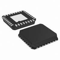
AD7626BCPZ Analog Devices Inc, AD7626BCPZ Datasheet - Page 4

AD7626BCPZ
Manufacturer Part Number
AD7626BCPZ
Description
IC ADC 16BIT 10MSPS DIFF 32LFCSP
Manufacturer
Analog Devices Inc
Datasheet
1.AD7626BCPZ-RL7.pdf
(28 pages)
Specifications of AD7626BCPZ
Data Interface
Serial
Design Resources
Single-Ended-to-Differential High Speed Drive Circuit for 16-Bit, 10 MSPS AD7626 ADC (CN0105)
Number Of Bits
16
Sampling Rate (per Second)
10M
Number Of Converters
1
Power Dissipation (max)
170mW
Voltage Supply Source
Single Supply
Operating Temperature
-40°C ~ 85°C
Mounting Type
Surface Mount
Package / Case
32-VFQFN, CSP Exposed Pad
Resolution (bits)
16bit
Sampling Rate
10MSPS
Input Channel Type
Differential
Supply Current
23.5mA
Digital Ic Case Style
CSP
No. Of Pins
32
Lead Free Status / RoHS Status
Lead free / RoHS Compliant
Available stocks
Company
Part Number
Manufacturer
Quantity
Price
Company:
Part Number:
AD7626BCPZ
Manufacturer:
ADI
Quantity:
263
Part Number:
AD7626BCPZ
Manufacturer:
ADI/亚德诺
Quantity:
20 000
Company:
Part Number:
AD7626BCPZ-RL7
Manufacturer:
PERICOM
Quantity:
101
Part Number:
AD7626BCPZ-RL7
Manufacturer:
ADI/亚德诺
Quantity:
20 000
AD7626
Parameter
REFERENCE BUFFER
EXTERNAL REFERENCE
VCM PIN
LVDS I/O (ANSI-644)
POWER SUPPLIES
TEMPERATURE RANGE
1
2
3
Using an external reference.
The ANSI-644 LVDS specification has a minimum output common mode (V
Power dissipation is for the AD7626 device only. In self-clocked interface mode, 0.9 mW is dissipated in the 100 Ω terminator. In echoed-clock interface mode, 1.8 mW
is dissipated in two 100 Ω terminators.
REFIN Input Voltage Range
REF Output Voltage Range
Line Regulation
Voltage Range
VCM Output
VCM Error
Output Impedance
Data Format
Differential Output Voltage, V
Common-Mode Output Voltage, V
Differential Input Voltage, V
Common-Mode Input Voltage, V
Specified Performance
Operating Currents
Power Dissipation
Energy per Conversion
Specified Performance
Power-Down
VDD1
VDD2
VIO
Static—Not Converting
With Internal Reference
With External Reference
Static—Not Converting
With Internal Reference
With External Reference
Power-Down
VDD1
VDD2
VIO
VDD1
VDD2
VIO
VDD1
VDD2
VIO
VDD1
VDD2
VIO
3
ID
OD
ICM
OCM
Test Conditions/Comments
REF @ 25°C, EN0 = EN1 = 1
VDD1 ± 5%, VDD2 ± 5%
REF
R
R
10 MSPS throughput
Echoed-clock mode
10 MSPS throughput
Echoed-clock mode
EN0 = 0, EN1 = 0
10 MSPS throughput
10 MSPS throughput
10 MSPS throughput
T
MIN
L
L
= 100 Ω
= 100 Ω
to T
MAX
Rev. A | Page 4 of
OCM
) of 1125 mV.
Min
1.18
4.076
−0.015
245
980
100
800
4.75
2.37
2.37
−40
2
Serial LVDS twos complement
Typ
1.2
4.096
5
4.096
REF/2
5
290
1130
5
2.5
2.5
3.5
16.7
11.6
10.4
23.5
15.8
7.5
23
16.4
0.6
0.8
1
88
150
136
8
13.6
Max
1.22
4.116
+0.015
454
1375
650
1575
5.25
2.63
2.63
4.5
21.2
13.5
11.2
27.8
17.8
8.8
28
18.5
4
10
5
107
170
160
58
+85
Unit
V
V
mV
V
V
kΩ
mV
mV
mV
mV
V
V
V
mA
mA
mA
mA
mA
mA
mA
mA
mA
μA
μA
μA
mW
mW
mW
μW
nJ/sample
°C


