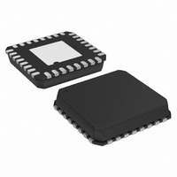
AD7626BCPZ Analog Devices Inc, AD7626BCPZ Datasheet - Page 24

AD7626BCPZ
Manufacturer Part Number
AD7626BCPZ
Description
IC ADC 16BIT 10MSPS DIFF 32LFCSP
Manufacturer
Analog Devices Inc
Datasheet
1.AD7626BCPZ-RL7.pdf
(28 pages)
Specifications of AD7626BCPZ
Data Interface
Serial
Design Resources
Single-Ended-to-Differential High Speed Drive Circuit for 16-Bit, 10 MSPS AD7626 ADC (CN0105)
Number Of Bits
16
Sampling Rate (per Second)
10M
Number Of Converters
1
Power Dissipation (max)
170mW
Voltage Supply Source
Single Supply
Operating Temperature
-40°C ~ 85°C
Mounting Type
Surface Mount
Package / Case
32-VFQFN, CSP Exposed Pad
Resolution (bits)
16bit
Sampling Rate
10MSPS
Input Channel Type
Differential
Supply Current
23.5mA
Digital Ic Case Style
CSP
No. Of Pins
32
Lead Free Status / RoHS Status
Lead free / RoHS Compliant
Available stocks
Company
Part Number
Manufacturer
Quantity
Price
Company:
Part Number:
AD7626BCPZ
Manufacturer:
ADI
Quantity:
263
Part Number:
AD7626BCPZ
Manufacturer:
ADI/亚德诺
Quantity:
20 000
Company:
Part Number:
AD7626BCPZ-RL7
Manufacturer:
PERICOM
Quantity:
101
Part Number:
AD7626BCPZ-RL7
Manufacturer:
ADI/亚德诺
Quantity:
20 000
AD7626
APPLICATIONS INFORMATION
LAYOUT, DECOUPLING, AND GROUNDING
When laying out the printed circuit board (PCB) for the AD7626,
follow the practices described in this section to obtain the maxi-
mum performance from the converter.
Exposed Paddle
The AD7626 has an exposed paddle on the underside of the
package.
•
•
•
•
VDD1 Supply Routing and Decoupling
The VDD1 supply is connected to Pin 1, Pin 19, and Pin 20.
Decouple the supply using a 100 nF capacitor at Pin 1. The user
can connect this supply trace to Pin 19 and Pin 20. Use a series
ferrite bead to connect the VDD1 supply from Pin 1 to Pin 19
and Pin 20. The ferrite bead isolates any high frequency noise or
ringing on the VDD1 supply. Decouple the VDD1 supply to Pin
19 and Pin 20 using a 100 nF capacitor decoupled to ground at
the exposed paddle.
Solder the paddle directly to the PCB.
Connect the paddle to the ground plane of the board using
multiple vias, as shown in Figure 43.
Decouple all supply pins except for Pin 12 (VIO) directly to
the paddle, minimizing the current return path.
Pin 13 and Pin 24 can be connected directly to the paddle.
Use vias to ground at the point where these pins connect to
the paddle.
EXTERNAL REFERENCE
(ADR434 OR ADR444)
4.096V
Figure 43. PCB Layout and Decoupling Recommendations for Pin 24 to Pin 32
Rev. A | Page 24 of 2
VIO Supply Decoupling
Decouple the VIO supply applied to Pin 12 to ground at Pin 13.
Layout and Decoupling of Pin 25 to Pin 32
Connect the outputs of Pin 25, Pin 26, and Pin 28 together and
decouple them to Pin 27 using a 10 μF capacitor with low ESR
and low ESL.
Reduce the inductance of the path connecting Pin 25, Pin 26,
and Pin 28 by widening the PCB traces connecting these pins.
Take a similar approach in the connections used for the
reference pins of the AD7626. Connect Pin 29, Pin 30, and
Pin 32 together using widened PCB traces to reduce inductance.
In internal or external reference mode, a 4.096 V reference voltage
is output on Pin 29, Pin 30, and Pin 32. Decouple these pins to
Pin 31 using a 10 μF capacitor with low ESR and low ESL.
Figure 43 shows an example of the recommended layout for
the underside of the AD7626 device. Note the extended signal
trace connections and the outline of the capacitors decoupling
the signals applied to the REF pins (Pin 29, Pin 30, and Pin 32)
and to the CAP2 pins (Pin 25, Pin 26, and Pin 28).
25
26
27
28
29
30
31
32
24 23 22 21 20 19 18 17
1
2
3
PADDLE
4
5
6
7
8
16
15
14
13
12
11
10
9


