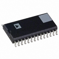
AD7863BR-3 Analog Devices Inc, AD7863BR-3 Datasheet - Page 7

AD7863BR-3
Manufacturer Part Number
AD7863BR-3
Description
IC ADC 14BIT DUAL 2CH 28-SOIC
Manufacturer
Analog Devices Inc
Datasheet
1.AD7863ARZ-3.pdf
(24 pages)
Specifications of AD7863BR-3
Rohs Status
RoHS non-compliant
Number Of Bits
14
Sampling Rate (per Second)
175k
Data Interface
Parallel
Number Of Converters
2
Power Dissipation (max)
94.5mW
Voltage Supply Source
Analog and Digital
Operating Temperature
-40°C ~ 85°C
Mounting Type
Surface Mount
Package / Case
28-SOIC (0.300", 7.50mm Width)
PIN CONFIGURATION AND FUNCTION DESCRIPTIONS
Table 4. Pin Function Descriptions
Pin
No.
1 to 6
7
8
9 to 15
16
17
18
19
20
21
22
23
24
25
26
27
28
DGND
CONVST
AGND
V
V
V
CS
RD
BUSY
V
V
V
AGND
DB13
Mnemonic
DB12 to DB7
DB6 to DB0
A0
B2
A2
REF
DD
A1
B1
Description
Data Bit 12 to Data Bit 7. Three-state TTL outputs.
Digital Ground. Ground reference for digital circuitry.
Convert Start Input. Logic input. A high-to-low transition on this input puts both track/holds into their hold mode
and starts conversion on both channels.
Data Bit 6 to Data Bit 0. Three-state TTL outputs.
Analog Ground. Ground reference for mux, track/hold, reference, and DAC circuitry.
Input Number 2 of Channel B. Analog input voltage ranges of ±10 V (AD7863-10), ±2.5 V (AD7863-3), and 0 V to
2.5 V (AD7863-2).
Input Number 2 of Channel A. Analog input voltage ranges of ±10 V (AD7863-10), ±2.5 V (AD7863-3), and 0 V to
2.5 V (AD7863-2).
Reference Input/Output. This pin is connected to the internal reference through a series resistor and is the output
reference source for the analog-to-digital converter. The nominal reference voltage is 2.5 V, and this appears at the pin.
Multiplexer Select. This input is used in conjunction with CONVST to determine on which pair of channels the
conversion is to be performed. If A0 is low when the conversion is initiated, then channels V
selected. If A0 is high when the conversion is initiated, channels V
Chip Select Input. Active low logic input. The device is selected when this input is active.
Read Input. Active low logic input. This input is used in conjunction with CS low to enable the data outputs and
read a conversion result from the AD7863.
Busy Output. The busy output is triggered high by the falling edge of CONVST and remains high until conversion
is completed.
Analog and Digital Positive Supply Voltage, 5.0 V ± 5%.
Input Number 1 of Channel A. Analog input voltage ranges of ±10 V (AD7863-10), ±2.5 V (AD7863-3), and 0 V to
2.5 V (AD7863-2).
Input Number 1 of Channel B. Analog input voltage ranges of ±10 V (AD7863-10), ±2.5 V (AD7863-3), and 0 V to
2.5 V (AD7863-2).
Analog Ground. Ground reference for mux, track/hold, reference, and DAC circuitry.
Data Bit 13 (MSB). Three-state TTL output. Output coding is twos complement for the AD7863-10 and AD7863-3.
Output coding is straight (natural) binary for the AD7863-2.
CONVST
DGND
DB12
DB11
DB10
DB9
DB8
DB7
DB6
DB5
DB4
DB3
DB2
DB1
Figure 4. Pin Configuration
Rev. B | Page 7 of 24
10
11
12
13
14
1
2
3
4
5
6
7
8
9
(Not to Scale)
AD7863
TOP VIEW
28
27
26
25
24
23
22
21
20
19
18
17
16
15
AGND
V
V
V
DB13
BUSY
RD
CS
A0
V
V
V
AGND
DB0
B1
A1
DD
REF
A2
B2
B1
and V
B2
are selected.
A1
and V
A2
AD7863
are


