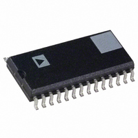
AD7863BR-3 Analog Devices Inc, AD7863BR-3 Datasheet - Page 11

AD7863BR-3
Manufacturer Part Number
AD7863BR-3
Description
IC ADC 14BIT DUAL 2CH 28-SOIC
Manufacturer
Analog Devices Inc
Datasheet
1.AD7863ARZ-3.pdf
(24 pages)
Specifications of AD7863BR-3
Rohs Status
RoHS non-compliant
Number Of Bits
14
Sampling Rate (per Second)
175k
Data Interface
Parallel
Number Of Converters
2
Power Dissipation (max)
94.5mW
Voltage Supply Source
Analog and Digital
Operating Temperature
-40°C ~ 85°C
Mounting Type
Surface Mount
Package / Case
28-SOIC (0.300", 7.50mm Width)
Gain error can be adjusted at either the first code transition (ADC
negative full scale) or the last code transition (ADC positive full
scale). The trim procedures for both cases are as follows:
Positive Full-Scale Adjust (−10 Version)
Apply a voltage of 9.9927 V (FS/2 – 1 LSBs) at V
until the ADC output code flickers between 01 1111 1111 1110
and 01 1111 1111 1111.
Negative Full-Scale Adjust (−10 Version)
Apply a voltage of −9.9976 V (−FS + 1 LSB) at V
until the ADC output code flickers between 10 0000 0000 0000
and 10 0000 0000 0001.
An alternative scheme for adjusting full-scale error in systems
that use an external reference is to adjust the voltage at the V
pin until the full-scale error for any of the channels is adjusted
out. The good full-scale matching of the channels ensures small
full-scale errors on the other channels.
TIMING AND CONTROL
Figure 7 shows the timing and control sequence required to
obtain optimum performance (Mode 1) from the AD7863. In
the sequence shown, a conversion is initiated on the falling edge
of CONVST . This places both track-and-holds into hold
simultaneously and new data from this conversion is available
in the output register of the AD7863 5.2 μs later. The BUSY
CONVST
BUSY
DATA
CS
RD
A0
t
CONV
t
Figure 7. Mode 1 Timing Operation Diagram for High Sampling Performance
3
= 5.2µs
t
1
t
5
1
1
. Adjust R2
. Adjust R2
V
t
4
A1
Rev. B | Page 11 of 24
REF
V
A2
t
ACQ
t
8
t
6
t
2
signal indicates the end of conversion and at this time the
conversion results for both channels are available to be read. A
second conversion is then initiated. If the multiplexer select (A0)
is low, the first and second read pulses after the first conversion
accesses the result from Channel A (V
The third and fourth read pulses, after the second conversion
and A0 high, accesses the result from Channel B (V
respectively). The state of A0 can be changed any time after the
CONVST goes high, that is, track-and-holds into hold and 500 ns
prior to the next falling edge of CONVST . Note that A0 should
not be changed during conversion if the nonselected channels
have negative voltages applied to them, which are outside the
input range of the AD7863, because this affects the conversion
in progress. Data is read from the part via a 14-bit parallel data
bus with standard CS and RD signal, that is, the read operation
consists of a negative going pulse on the CS pin combined with
two negative going pulses on the RD pin (while the CS is low),
accessing the two 14-bit results. Once the read operation has
taken place, a further 400 ns should be allowed before the next
falling edge of CONVST to optimize the settling of the track-
and-hold amplifier before the next conversion is initiated.
The achievable throughput rate for the part is 5.2 μs (conversion
time) plus 100 ns (read time) plus 0.4 μs (quiet time). This
results in a minimum throughput time of 5.7 μs (equivalent to
a throughput rate of 175 kHz).
V
B1
t
7
V
B2
A1
and V
A2
, respectively).
B1
AD7863
and V
B2
,


