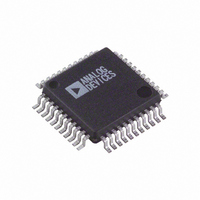
AD9240AS Analog Devices Inc, AD9240AS Datasheet - Page 17

AD9240AS
Manufacturer Part Number
AD9240AS
Description
IC ADC 14BIT 10MSPS 44-MQFP
Manufacturer
Analog Devices Inc
Datasheet
1.AD9240ASZ.pdf
(24 pages)
Specifications of AD9240AS
Mounting Type
Surface Mount
Rohs Status
RoHS non-compliant
Number Of Bits
14
Sampling Rate (per Second)
10M
Data Interface
Parallel
Number Of Converters
7
Power Dissipation (max)
330mW
Voltage Supply Source
Analog and Digital
Operating Temperature
-40°C ~ 85°C
Package / Case
44-MQFP, 44-PQFP
Power Dissipation Pd
330mW
Input Channels Per Adc
2
No. Of Channels
2
Peak Reflow Compatible (260 C)
No
Sample Rate
10MSPS
Supply Voltage Max
5V
No. Of Bits
14 Bit
For Use With
AD9240-EB - BOARD EVAL FOR AD9240
Lead Free Status / RoHS Status
Contains lead / RoHS non-compliant
Available stocks
Company
Part Number
Manufacturer
Quantity
Price
Company:
Part Number:
AD9240AS
Manufacturer:
AD
Quantity:
5 510
Part Number:
AD9240AS
Manufacturer:
ADI/亚德诺
Quantity:
20 000
Company:
Part Number:
AD9240ASRL
Manufacturer:
Analog Devices Inc
Quantity:
10 000
Company:
Part Number:
AD9240ASZ
Manufacturer:
ADI
Quantity:
850
Company:
Part Number:
AD9240ASZ
Manufacturer:
Analog Devices Inc
Quantity:
10 000
Part Number:
AD9240ASZ
Manufacturer:
ADI/亚德诺
Quantity:
20 000
Company:
Part Number:
AD9240ASZRL
Manufacturer:
MAXIM
Quantity:
495
the resultant VREF output is 2.5 V. The valid input range thus
becomes 0 V to 5 V. The VREF pin should be bypassed to the
REFCOM pin with a 10 F tantalum capacitor in parallel with a
low-inductance 0.1 F ceramic capacitor.
Single-Ended or Differential Input, V
Figure 37 shows the single-ended configuration that gives the
best SINAD performance. To optimize dynamic specifications,
center the common-mode voltage of the analog input at
approximately by 2.5 V by connecting VINB to VREF, a low-
impedance 2.5 V source. As described above, shorting the
SENSE pin directly to the REFCOM pin results in a 2.5 V
reference voltage and a 5 V p-p input span. The valid range
for input signals is 0 V to 5 V. The VREF pin should be by-
passed to the REFCOM pin with a 10 F tantalum capacitor in
parallel with a low inductance 0.1 F ceramic capacitor.
This reference configuration could also be used for a differential
input in which VINA and VINB are driven via a transformer as
shown in Figure 32. In this case, the common-mode voltage,
V
tap to CML of the AD9240. VREF can be configured for 1 V
or 2.5 V by connecting SENSE to either VREF or REFCOM
respectively. Note that the valid input range for each of the
differential inputs is one half of the single-ended input and thus
becomes V
Resistor Programmable Reference
Figure 41 shows an example of how to generate a reference
voltage other than 1 V or 2.5 V with the addition of two external
resistors and a bypass capacitor. Use the equation,
to determine appropriate values for R1 and R2. These resistors
should be in the 2 k to 100 k range. For the example
shown, R1 equals 2.5 k and R2 equals 5 k . From the equa-
tion above, the resultant reference voltage on the VREF pin is
1.5 V. This sets the input span to be 3 V p-p. To assure stabil-
ity, place a 0.1 F ceramic capacitor in parallel with R1.
The common-mode voltage can be set to VREF by connecting
VINB to VREF to provide an input span of 0 to 2
Alternatively, the common-mode voltage can be set to 2.5 V
by connecting VINB to a low impedance 2.5 V source. For
REV.
CM
Figure 40. Internal Reference—5 V p-p Input Span,
V
CM
, is set at midsupply by connecting the transformer’s center
B
= 2.5 V
CM
5V
0V
– VREF/2 to V
10 F
VREF = 1 V
0.1 F
CM
2.5V
+ VREF/2.
(1 + R1/R2),
VINA
VINB
VREF
SENSE
REFCOM
CM
= 2.5 V
AD9240
VREF.
–17–
the example shown, the valid input signal range for VINA is 1 V
to 4 V since VINB is set to an external, low impedance 2.5 V
source. The VREF pin should be bypassed to the REFCOM pin
with a 10 F tantalum capacitor in parallel with a low induc-
tance 0.1 F ceramic capacitor.
USING AN EXTERNAL REFERENCE
Using an external reference may enhance the dc performance of
the AD9240 by improving drift and accuracy. Figures 42
through 44 show examples of how to use an external reference
with the A/D. Table III is a list of suitable voltage references
from Analog Devices. To use an external reference, the user
must disable the internal reference amplifier and drive the
VREF pin. Connecting the SENSE pin to AVDD disables the
internal reference amplifier.
Internal
REF191
Internal
REF192
AD780
The AD9240 contains an internal reference buffer, A2 (see
Figure 29), that simplifies the drive requirements of an external
reference. The external reference must be able to drive a 5 k
( 20%) load. Note that the bandwidth of the reference buffer is
deliberately left small to minimize the reference noise contribu-
tion. As a result, it is not possible to change the reference volt-
age rapidly in this mode without the removal of the CAPT/
CAPB Decoupling Network, and driving these pins directly.
Figure 41. Resistor Programmable Reference (3 V p-p
Input Span, V
4V
10 F
1V
2.5V
Output
Voltage
1.00
2.048
2.50
2.50
2.50
Table III. Suitable Voltage References
CM
0.1 F
= 2.5 V)
Drift
(ppm/ C)
26
5–25
26
5–25
3–7
R1
2.5k
R2
5k
C1
0.1 F
1.5V
Initial
Accuracy
% (max)
1.4
0.1–0.5
1.4
0.08–0.4
0.04–0.2
VINA
VINB
VREF
SENSE
REFCOM
AD9240
AD9240
Operating
Current
N/A
45
N/A
45
1000
( A)


