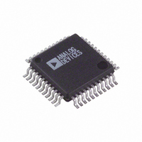
AD9240AS Analog Devices Inc, AD9240AS Datasheet - Page 12

AD9240AS
Manufacturer Part Number
AD9240AS
Description
IC ADC 14BIT 10MSPS 44-MQFP
Manufacturer
Analog Devices Inc
Datasheet
1.AD9240ASZ.pdf
(24 pages)
Specifications of AD9240AS
Mounting Type
Surface Mount
Rohs Status
RoHS non-compliant
Number Of Bits
14
Sampling Rate (per Second)
10M
Data Interface
Parallel
Number Of Converters
7
Power Dissipation (max)
330mW
Voltage Supply Source
Analog and Digital
Operating Temperature
-40°C ~ 85°C
Package / Case
44-MQFP, 44-PQFP
Power Dissipation Pd
330mW
Input Channels Per Adc
2
No. Of Channels
2
Peak Reflow Compatible (260 C)
No
Sample Rate
10MSPS
Supply Voltage Max
5V
No. Of Bits
14 Bit
For Use With
AD9240-EB - BOARD EVAL FOR AD9240
Lead Free Status / RoHS Status
Contains lead / RoHS non-compliant
Available stocks
Company
Part Number
Manufacturer
Quantity
Price
Company:
Part Number:
AD9240AS
Manufacturer:
AD
Quantity:
5 510
Part Number:
AD9240AS
Manufacturer:
ADI/亚德诺
Quantity:
20 000
Company:
Part Number:
AD9240ASRL
Manufacturer:
Analog Devices Inc
Quantity:
10 000
Company:
Part Number:
AD9240ASZ
Manufacturer:
ADI
Quantity:
850
Company:
Part Number:
AD9240ASZ
Manufacturer:
Analog Devices Inc
Quantity:
10 000
Part Number:
AD9240ASZ
Manufacturer:
ADI/亚德诺
Quantity:
20 000
Company:
Part Number:
AD9240ASZRL
Manufacturer:
MAXIM
Quantity:
495
AD9240
REFERENCE OPERATION
The AD9240 contains an onboard bandgap reference that pro-
vides a pin-strappable option to generate either a 1 V or 2.5 V
output. With the addition of two external resistors, the user can
generate reference voltages other than 1 V and 2.5 V. Another
alternative is to use an external reference for designs requiring
enhanced accuracy and/or drift performance. See Table II for a
summary of the pin-strapping options for the AD9240 reference
configurations.
Figure 29 shows a simplified model of the internal voltage
reference of the AD9240. A pin-strappable reference ampli-
fier buffers a 1 V fixed reference. The output from the refer-
ence amplifier, A1, appears on the VREF pin. The voltage on
the VREF pin determines the full-scale input span of the A/D.
This input span equals,
The voltage appearing at the VREF pin as well as the state of
the internal reference amplifier, A1, are determined by the volt-
age appearing at the SENSE pin. The logic circuitry contains
two comparators which monitor the voltage at the SENSE pin.
The comparator with the lowest set point (approximately 0.3 V)
controls the position of the switch within the feedback path of
A1. If the SENSE pin is tied to REFCOM, the switch is con-
nected to the internal resistor network thus providing a VREF of
2.5 V. If the SENSE pin is tied to the VREF pin via a short or
resistor, the switch is connected to the SENSE pin. A short will
provide a VREF of 1.0 V while an external resistor network will
provide an alternative VREF between 1.0 V and 2.5 V.
The second comparator controls internal circuitry that will
disable the reference amplifier if the SENSE pin is tied AVDD.
Disabling the reference amplifier allows the VREF pin to be
driven by an external voltage reference.
Figure 29. Equivalent Reference Circuit
A/D
TO
Full-Scale Input Span = 2 VREF
DISABLE
DISABLE
5k
5k
1V
A1
A2
AD9240
A2
A1
5k
5k
LOGIC
LOGIC
7.5k
5k
CAPT
CAPB
VREF
SENSE
REFCOM
–12–
The actual reference voltages used by the internal circuitry of
the AD9240 appear on the CAPT and CAPB pins. For proper
operation when using the internal or an external reference, it is
necessary to add a capacitor network to decouple these pins.
Figure 30 shows the recommended decoupling network. This
capacitive network performs the following three functions: (1)
along with the reference amplifier, A2, it provides a low source
impedance over a large frequency range to drive the A/D inter-
nal circuitry, (2) it provides the necessary compensation for A2
and (3) it bandlimits the noise contribution from the reference.
The turn-on time of the reference voltage appearing between
CAPT and CAPB is approximately 15 ms and should be evalu-
ated in any power-down mode of operation.
The A/D’s input span may be varied dynamically by changing
the differential reference voltage appearing across CAPT and
CAPB symmetrically around 2.5 V (i.e., midsupply). To change
the reference at speeds beyond the capabilities of A2, it will be
necessary to drive CAPT and CAPB with two high speed, low
noise amplifiers. In this case, both internal amplifiers (i.e., A1
and A2) must be disabled by connecting SENSE to AVDD and
VREF to REFCOM and the capacitive decoupling network
removed. The external voltages applied to CAPT and CAPB
must be 2.5 V + Input Span/4 and 2.5 V – Input Span/4, respec-
tively, where the input span can be varied between 2 V and 5 V.
Note that those samples within the pipeline A/D during any
reference transition will be corrupted and should be discarded.
Figure 30. Recommended CAPT/CAPB Decoupling Network
AD9240
CAPT
CAPB
0.1 F
10 F
0.1 F
0.1 F
REV.
B


