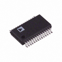
AD9059BRS Analog Devices Inc, AD9059BRS Datasheet - Page 9

AD9059BRS
Manufacturer Part Number
AD9059BRS
Description
IC ADC 8BIT DUAL 60MSPS 28-SSOP
Manufacturer
Analog Devices Inc
Datasheet
1.AD9059BRSZ-REEL.pdf
(12 pages)
Specifications of AD9059BRS
Mounting Type
Surface Mount
Package / Case
28-SSOP (0.200", 5.30mm Width)
Rohs Status
RoHS non-compliant
Number Of Bits
8
Sampling Rate (per Second)
60M
Data Interface
Parallel
Number Of Converters
2
Power Dissipation (max)
505mW
Voltage Supply Source
Analog and Digital
Operating Temperature
-40°C ~ 85°C
Peak Reflow Compatible (260 C)
No
No. Of Bits
8 Bit
Leaded Process Compatible
No
Features
Dual-Channel
No. Of Channels
2
Interface Type
Serial
Lead Free Status / RoHS Status
Contains lead / RoHS non-compliant
Available stocks
Company
Part Number
Manufacturer
Quantity
Price
Company:
Part Number:
AD9059BRS
Manufacturer:
AD
Quantity:
5 510
Company:
Part Number:
AD9059BRS
Manufacturer:
ADI
Quantity:
242
Part Number:
AD9059BRS
Manufacturer:
AD
Quantity:
20 000
Part Number:
AD9059BRS-REEL
Manufacturer:
ADI/亚德诺
Quantity:
20 000
Part Number:
AD9059BRSZ
Manufacturer:
ADI/亚德诺
Quantity:
20 000
Evaluation Board
The AD9059/PCB evaluation board provides an easy-to-use
analog/digital interface for the dual 8-bit, 60 MSPS ADC. The
board includes typical hardware configurations for a variety of high
speed digitization evaluations. On-board components include the
AD9059 (in the 28-lead SSOP package), optional analog input
buffer amplifiers, digital output latches, board timing drivers, and
configurable jumpers for ac coupling, dc coupling, and power-
down function testing. The board is configured at shipment for
dc coupling using the AD9059’s internal reference.
For dc-coupled analog input applications, amplifiers U3 and U4
are configured to operate as unity gain inverters with adjustable
offset for the analog input signals. For full-scale ADC drive,
each analog input signal should be 1 V p-p into 50 Ω referenced
to ground. Each amplifier offsets its analog signal by +VREF
(2.5 V typical) to center the voltage for proper ADC input drive.
For dc-coupled operation, connect E7 to E9 (analog input A to
R11), E14 to E13 (amplifier output to analog input A of
AD9059), E4 to E5 (analog input B to R10), and E11 to E10
(amplifier output to analog input B of AD9059) using the board
jumper connectors.
For ac-coupled analog input applications, amplifiers U3 and U4
are removed from the analog signal paths. The analog signals
are coupled through Capacitors C11 and C12, each terminated
to the VREF voltage through separate 1 kΩ resistors (providing
bias current for the AD9059 analog inputs, AINA and AINB).
REV. A
2.5V
VOLTAGE REFERENCE
800
+V
D
3k
2.5k
VREF
ENCODE
PWRDN
DIGITAL INPUTS
Figure 6. Equivalent Circuits
+V
D
–9–
DIGITAL OUTPUTS
Analog input signals to the board should be 1 V p-p into 50 Ω
for full-scale ADC drive. For ac-coupled operation, connect E7
to E8 (analog input A to C12 feedthrough capacitor), E13 to
E15 (C12 to R15 termination resistor for Channel A), E4 to E6
(analog input B to C11 feedthrough capacitor), and E10 to E12
(C11 to R14 termination resistor for Channel B) using the
board jumper connectors.
The on-board reference voltage may be used to drive the ADC or
an external reference may be applied. The standard configuration
employs the internal voltage reference without any external
connection requirements. An external voltage reference may be
applied at board connector input REF to overdrive the limited
current output of the AD9059’s internal voltage reference. The
external voltage reference should be 2.5 V typical.
The power-down function of the AD9059 can be exercised
through a board jumper connection. Connect E2 to E1 (5 V to
PWRDN) for power-down mode operation. For normal operation,
connect E3 to E1 (ground to PWRDN).
The encode signal source should be TTL/CMOS compatible
and capable of driving a 50 Ω termination. The digital outputs
of the AD9059 are buffered through latches on the evaluation
board (U5 and U6) and are available for the user at connector
Pins 30–37 and Pins 22–29. Latch timing is derived from the
ADC ENCODE clock and a digital clocking signal is provided
for the board user at connector Pins 2 and 21.
3V TO 5V
+V
DD
D0–D7
AIN
ANALOG INPUTS
500
+V
D
AD9059
VREF


