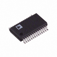
AD9059BRS Analog Devices Inc, AD9059BRS Datasheet - Page 3

AD9059BRS
Manufacturer Part Number
AD9059BRS
Description
IC ADC 8BIT DUAL 60MSPS 28-SSOP
Manufacturer
Analog Devices Inc
Datasheet
1.AD9059BRSZ-REEL.pdf
(12 pages)
Specifications of AD9059BRS
Mounting Type
Surface Mount
Package / Case
28-SSOP (0.200", 5.30mm Width)
Rohs Status
RoHS non-compliant
Number Of Bits
8
Sampling Rate (per Second)
60M
Data Interface
Parallel
Number Of Converters
2
Power Dissipation (max)
505mW
Voltage Supply Source
Analog and Digital
Operating Temperature
-40°C ~ 85°C
Peak Reflow Compatible (260 C)
No
No. Of Bits
8 Bit
Leaded Process Compatible
No
Features
Dual-Channel
No. Of Channels
2
Interface Type
Serial
Lead Free Status / RoHS Status
Contains lead / RoHS non-compliant
Available stocks
Company
Part Number
Manufacturer
Quantity
Price
Company:
Part Number:
AD9059BRS
Manufacturer:
AD
Quantity:
5 510
Company:
Part Number:
AD9059BRS
Manufacturer:
ADI
Quantity:
242
Part Number:
AD9059BRS
Manufacturer:
AD
Quantity:
20 000
Part Number:
AD9059BRS-REEL
Manufacturer:
ADI/亚德诺
Quantity:
20 000
Part Number:
AD9059BRSZ
Manufacturer:
ADI/亚德诺
Quantity:
20 000
SPECIFICATIONS
Parameter
DIGITAL INPUTS
DIGITAL OUTPUTS
POWER SUPPLY
NOTES
1
2
3
4
5
6
Specifications subject to change without notice.
EXPLANATION OF TEST LEVELS
Test Level
I
II – 100% production tested at +25°C and sample tested at
III – Sample tested only.
IV – Parameter is guaranteed by design and characterization
V – Parameter is a typical value only.
VI – 100% production tested at +25°C; guaranteed by design
CAUTION
ESD (electrostatic discharge) sensitive device. Electrostatic charges as high as 4000 V readily
accumulate on the human body and test equipment and can discharge without detection. Although the
AD9059 features proprietary ESD protection circuitry, permanent damage may occur on devices
subjected to high energy electrostatic discharges. Therefore, proper ESD precautions are recommended
to avoid performance degradation or loss of functionality.
REV. A
Gain error and gain temperature coefficient are based on the ADC only (with a fixed 2.5 V external reference).
t
SNR/harmonics based on an analog input voltage of –0.5 dBFS referenced to a 1.0 V full-scale input range.
Digital supply current based on V
Power dissipation is based on 60 MSPS encode and 10.3 MHz analog input dynamic test conditions (V
Typical thermal impedance for the RS style (SSOP) 28-lead package: θ
an ac load of 10 pF or a dc current of ± 40 µA.
V
Logic 1 Voltage
Logic 0 Voltage
Logic 1 Current
Logic 0 Current
Input Capacitance
Encode Pulsewidth High (t
Encode Pulsewidth Low (t
Logic 1 Voltage (V
Logic 1 Voltage (V
Logic 0 Voltage (V
Output Coding
V
V
Power Dissipation
Power-Down Dissipation
Power Supply Rejection Ratio (PSRR)
and t
– 100% production tested.
D
DD
Supply Current (V
PD
Supply Current (V
specified temperatures.
testing.
and characterization testing for industrial temperature range.
are measured from the 1.5 V level of the ENCODE to the 10%/90% levels of the digital output swing. The digital output load during test is not to exceed
5, 6
DD
DD
DD
= 3 V)
= 5 V)
= 3 V or 5 V)
D
DD
= 5 V)
DD
EL
= 3 V)
EH
= 3 V output drive with <10 pF loading under dynamic test conditions.
)
)
(continued)
4
Temp
Full
Full
Full
25°C
25°C
25°C
Full
Full
Full
Full
Full
Full
25°C
Full
Full
JC
= 39°C/W, θ
–3–
ABSOLUTE MAXIMUM RATINGS*
V
Analog Inputs . . . . . . . . . . . . . . . . . . . . . . . –0.5 V to V
Digital Inputs . . . . . . . . . . . . . . . . . . . . . . . –0.5 V to V
VREF Input . . . . . . . . . . . . . . . . . . . . . . . . . –0.5 V to V
Digital Output Current . . . . . . . . . . . . . . . . . . . . . . . . . . . 20 mA
Operating Temperature . . . . . . . . . . . . . . . . . . –55°C to +125°C
Storage Temperature . . . . . . . . . . . . . . . . . . . . –65°C to +150°C
*Stresses above those listed under Absolute Maximum Ratings may cause permanent
Model
AD9059BRS
AD9059/PCB
damage to the device. This is a stress rating only; functional operation of the device
at these or any other conditions above those indicated in the operational sections of
this specification is not implied. Exposure to absolute maximum ratings for extended
periods may affect device reliability.
D
CA
, V
= 70°C/W, and θ
DD
Test Level
VI
VI
VI
VI
V
IV
IV
VI
IV
VI
VI
VI
VI
VI
I
. . . . . . . . . . . . . . . . . . . . . . . . . . . . . . . . . . . . . . . . 7 V
D
= 5 V ± 5%, V
Temperature Range
–40°C to +85°C
25°C
JA
= 109°C/W.
ORDERING GUIDE
Min
2.0
6.7
6.7
2.95
4.95
Offset Binary Code
DD
AD9059BRS
= 3 V ± 5%).
Typ
4.5
72
13
400
6
3
Max
0.8
± 1
± 1
166
166
0.05
92
15
505
12
Package Option
RS-28
Evaluation Board
mA
mA
Unit
V
V
µA
µA
pF
ns
ns
V
V
V
mW
mW
mV/V
AD9059
D
D
D
+ 0.5 V
+ 0.5 V
+ 0.5 V


