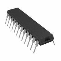
AD7892AN-1 Analog Devices Inc, AD7892AN-1 Datasheet - Page 4

AD7892AN-1
Manufacturer Part Number
AD7892AN-1
Description
IC ADC 12BIT LP 500KSPS 24-DIP
Manufacturer
Analog Devices Inc
Datasheet
1.AD7892BNZ-1.pdf
(14 pages)
Specifications of AD7892AN-1
Mounting Type
Through Hole
Package / Case
24-DIP (0.300", 7.62mm)
Rohs Status
RoHS non-compliant
Number Of Bits
12
Sampling Rate (per Second)
500k
Data Interface
Serial, Parallel
Number Of Converters
1
Power Dissipation (max)
90mW
Voltage Supply Source
Single Supply
Operating Temperature
-40°C ~ 85°C
No. Of Bits
12 Bit
Features
Single Supply, 12?Bit, 500kSPS ADC
No. Of Channels
1
Interface Type
Parallel
Number Of Elements
1
Resolution
12Bit
Architecture
SAR
Sample Rate
500KSPS
Input Polarity
Bipolar
Input Type
Voltage
Rated Input Volt
±5/±10V
Differential Input
No
Power Supply Requirement
Single
Single Supply Voltage (typ)
5V
Single Supply Voltage (min)
4.75V
Single Supply Voltage (max)
5.25V
Dual Supply Voltage (typ)
Not RequiredV
Dual Supply Voltage (min)
Not RequiredV
Dual Supply Voltage (max)
Not RequiredV
Power Dissipation
90mW
Differential Linearity Error
±1LSB
Integral Nonlinearity Error
±1.5LSB
Operating Temp Range
-40C to 85C
Operating Temperature Classification
Industrial
Mounting
Through Hole
Pin Count
24
Package Type
PDIP
Input Signal Type
Single-Ended
Lead Free Status / Rohs Status
Not Compliant
AD7892
TIMING CHARACTERISTICS
Parameter
t
t
Parallel Interface
t
t
t
t
t
t
t
t
t
Serial Interface
t
t
t
t
t
t
t
t
t
NOTES
1
2
3
4
5
Specifications subject to change without notice.
CAUTION
ESD (electrostatic discharge) sensitive device. Electrostatic charges as high as 4000 V readily
accumulate on the human body and test equipment and can discharge without detection.
Although the AD7892 features proprietary ESD protection circuitry, permanent damage may
occur on devices subjected to high energy electrostatic discharges. Therefore, proper ESD
precautions are recommended to avoid performance degradation or loss of functionality.
Sample tested at +25°C to ensure compliance. All input signals are measured with tr = tf = 1 ns (10% to 90% of +5 V) and timed from a voltage level of +1.6 V.
See Figures 2 and 3.
Measured with the load circuit of Figure 1 and defined as the time required for an output to cross 0.8 V or 2.4 V.
These times are derived from the measured time taken by the data outputs to change 0.5 V when loaded with the circuit of Figure 1. The measured number is then
Assumes CMOS loads on the data bits. With TTL loads, more current is drawn from the data lines and the RD to CONVST time needs to be extended to 400 ns min.
CONV
ACQ
1
2
3
4
5
6
7
8
9
10
11
12
13
14
15
16
17
17A
extrapolated back to remove the effects of charging or discharging the 50 pF capacitor. This means that the times quoted in the timing characteristics are the true bus
relinquish times of the part and as such are independent of external bus loading capacitances.
3
4
3
3
3
4
4
A, B
Versions
1.47
1.6
200
400
35
60
0
0
35
35
5
30
0
200
30
25
25
25
5
25
20
0
30
0
30
1, 2
(V
DD
S
Version
1.68
320
45
60
0
0
45
40
5
40
0
200
35
30
25
25
5
30
30
0
30
0
30
= +5 V
TO
OUTPUT
PIN
50pF
5%, AGND = DGND = 0 V, REF IN = +2.5 V)
Unit
µs max
µs max
ns min
ns min
ns min
ns min
ns min
ns min
ns min
ns max
ns min
ns max
ns min
ns min
ns min
ns max
ns min
ns min
ns min
ns max
ns min
ns min
ns max
ns min
ns max
1.6mA
200 A
+1.6V
Test Conditions/Comments
Conversion Time for AD7892-3
Conversion Time for AD7892-1, AD7892-2
Acquisition Time for AD7892-3
Acquisition Time for AD7892-1, AD7892-2
CONVST Pulsewidth
EOC Pulsewidth
EOC Falling Edge to CS Falling Edge Setup Time
CS to RD Setup Time
Read Pulsewidth
Data Access Time After Falling Edge of RD
Bus Relinquish Time After Rising Edge of RD
CS to RD Hold Time
RD to CONVST Setup Time
RFS Low to SCLK Falling Edge Setup Time
RFS Low to Data Valid Delay
SCLK High Pulsewidth
SCLK Low Pulsewidth
SCLK Rising Edge to Data Valid Hold Time
SCLK Rising Edge to Data Valid Delay
RFS to SCLK Falling Edge Hold Time
Bus Relinquish Time after Rising Edge of RFS
Bus Relinquish Time after Rising Edge of SCLK
WARNING!
ESD SENSITIVE DEVICE


