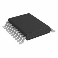
AD7997BRUZ-0 Analog Devices Inc, AD7997BRUZ-0 Datasheet - Page 19

AD7997BRUZ-0
Manufacturer Part Number
AD7997BRUZ-0
Description
IC ADC 10BIT 8CHAN I2C 20TSSOP
Manufacturer
Analog Devices Inc
Datasheet
1.AD7997BRUZ-1.pdf
(32 pages)
Specifications of AD7997BRUZ-0
Data Interface
I²C, Serial
Number Of Bits
10
Sampling Rate (per Second)
188k
Number Of Converters
1
Power Dissipation (max)
2.2mW
Voltage Supply Source
Single Supply
Operating Temperature
-40°C ~ 85°C
Mounting Type
Surface Mount
Package / Case
20-TSSOP (0.173", 4.40mm Width)
Resolution (bits)
10bit
Sampling Rate
188kSPS
Input Channel Type
Single Ended
Supply Voltage Range - Analog
2.7V To 5.5V
Supply Current
1.4mA
Number Of Elements
1
Resolution
10Bit
Architecture
SAR
Sample Rate
188KSPS
Input Polarity
Unipolar
Input Type
Voltage
Rated Input Volt
2.5V
Differential Input
No
Power Supply Requirement
Single
Single Supply Voltage (typ)
3.3/5V
Single Supply Voltage (min)
2.7V
Single Supply Voltage (max)
5.5V
Dual Supply Voltage (typ)
Not RequiredV
Dual Supply Voltage (min)
Not RequiredV
Dual Supply Voltage (max)
Not RequiredV
Power Dissipation
6.05mW
Differential Linearity Error
±0.5LSB
Integral Nonlinearity Error
±0.5LSB
Operating Temp Range
-40C to 85C
Operating Temperature Classification
Industrial
Mounting
Surface Mount
Pin Count
20
Package Type
TSSOP
Input Signal Type
Single-Ended
Lead Free Status / RoHS Status
Lead free / RoHS Compliant
For Use With
EVAL-AD7997CBZ - BOARD EVALUATION AD7997
Lead Free Status / Rohs Status
Compliant
Available stocks
Company
Part Number
Manufacturer
Quantity
Price
Part Number:
AD7997BRUZ-0
Manufacturer:
ADI/亚德诺
Quantity:
20 000
CONFIGURATION REGISTER
The configuration register is a 16-bit read/write register that is used to set the operating mode of the AD7997/AD7998. The 4 MSBs of the
register are unused. The bit functions of all 12 LSBs of the configuration register are outlined in Table 9. A 2-byte write is necessary when
writing to the configuration register.
Table 9. Configuration Register Bits and Default Settings at Power-Up
D15
DONTC
0
Table 10. Bit Function Descriptions
Bit
D11 to D4
D3
D2
D1
D0
Table 11. Channel Selection
D11
0
0
0
0
0
0
0
1
Table 12. ALERT/BUSY Function
D2
0
0
1
1
D10
0
0
0
0
0
0
1
0
D14
DONTC
0
D1
0
1
0
1
Mnemonic
CH8 to CH1
FLTR
ALERT EN
BUSY/ALERT
BUSY/ALERT
POLARITY
D9
0
0
0
0
0
1
0
0
D13
DONTC
0
ALERT/BUSY Pin Configuration
Pin does not provide any interrupt signal.
Pin configured as a BUSY output.
Pin configured as an ALERT output.
Resets the ALERT output pin, the Alert_Flag bit in the conversion result register, and the entire alert status register
(if any is active). If 1/1 is written to Bits D2/D1 in the configuration register to reset the ALERT pin, the Alert_Flag bit,
and the alert status register, the contents of the configuration register read 1/0 for D2/D1, respectively, if read back.
D8
0
0
0
0
1
0
0
0
Comment
These 8-channel address bits select the analog input channel(s) to be converted. A 1 in any of Bits D11 to D4
selects a channel for conversion. If more than one channel bit is set to 1, the AD7997/AD7998 sequence
through the selected channels, starting with the lowest channel. All unused channels should be set to 0. Prior
to initiating a conversion, a channel or channels for conversion must be selected in the configuration register.
The value written to this bit of the control register determines whether the filtering on SDA and SCL is
enabled or is to be bypassed. If this bit is a 1, then the filtering is enabled; if it is a 0, the filtering is bypassed.
The hardware ALERT function is enabled if this bit is set to 1, and disabled if this bit is set to 0. This bit is used
in conjunction with the BUSY/ALERT bit to determine if the ALERT/BUSY pin acts as an ALERT or a BUSY
output (see Table 12).
This bit is used in conjunction with the ALERT EN bit to determine if the ALERT/ BUSY output, Pin 17, acts as
an ALERT or BUSY output (see Table 12), and if Pin 17 is configured as an ALERT output pin, if it is to be reset.
This bit determines the active polarity of the ALERT/BUSY pin regardless of whether it is configured as an
ALERT or BUSY output. It is active low if this bit is set to 0, and active high if set to 1.
D12
DONTC
0
D7
0
0
0
1
0
0
0
0
D11
CH8
0
0
0
1
0
0
0
0
0
D6
D10
CH7
0
D5
0
1
0
0
0
0
0
0
D9
CH6
0
D4
1
0
0
0
0
0
0
0
Rev. 0 | Page 19 of 32
D8
CH5
0
Convert on Channel 1 (V
Convert on Channel 2 (V
Convert on Channel 3 (V
Convert on Channel 4 (V
Convert on Channel 5 (V
Convert on Channel 6 (V
Convert on Channel 7 (V
Convert on Channel 8 (V
Selected Analog Input Channel
D7
CH4
0
D6
CH3
0
D5
CH2
0
IN
IN
IN
IN
IN
IN
IN
IN
D4
CH1
0
1)
2)
3)
4)
5)
6)
7)
8)
D3
FLTR
1
Comments
If more than one channel is
selected, the AD7997/AD7998
start converting on the selected
sequence of channels starting with
the lowest channel in the
sequence.
D2
ALERT
EN
0
AD7997/AD7998
D1
BUSY/
ALERT
0
D0
ALERT/BUSY
POLARITY
0


