LTC2170IUKG-14#TRPBF Linear Technology, LTC2170IUKG-14#TRPBF Datasheet - Page 17
LTC2170IUKG-14#TRPBF
Manufacturer Part Number
LTC2170IUKG-14#TRPBF
Description
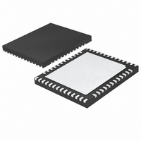
IC ADC 14BIT SER/PAR 25M 52-QFN
Manufacturer
Linear Technology
Datasheet
1.LTC2172IUKG-14PBF.pdf
(34 pages)
Specifications of LTC2170IUKG-14#TRPBF
Number Of Bits
14
Sampling Rate (per Second)
25M
Data Interface
Serial, Parallel
Number Of Converters
4
Power Dissipation (max)
243mW
Voltage Supply Source
Analog and Digital
Operating Temperature
-40°C ~ 85°C
Mounting Type
Surface Mount
Package / Case
52-WFQFN Exposed Pad
Lead Free Status / RoHS Status
Lead free / RoHS Compliant
Available stocks
Company
Part Number
Manufacturer
Quantity
Price


PIN FUNCTIONS
A
Input.
A
Input.
V
Equal to V
mode of the analog inputs of channels 1 and 2. Bypass
to ground with a 0.1μF ceramic capacitor.
A
Input.
A
Input.
REFH (Pins 6, 7): ADC High Reference. Bypass to Pin 8
and Pin 9 with a 2.2μF ceramic capacitor, and to ground
with a 0.1μF ceramic capacitor.
REFL (Pins 8, 9): ADC Low Reference. Bypass to Pin 6
and Pin 7 with a 2.2μF ceramic capacitor, and to ground
with a 0.1μF ceramic capacitor.
A
Input.
A
Input.
V
Equal to V
mode of the analog inputs of channels 3 and 4. Bypass
to ground with a 0.1μF ceramic capacitor.
A
Input.
A
Input.
V
Bypass to ground with 0.1μF ceramic capacitors. Adjacent
pins can share a bypass capacitor.
ENC
rising edge.
IN1
IN1
CM12
IN2
IN2
IN3
IN3
CM34
IN4
IN4
DD
+
–
+
–
+
–
+
–
+
(Pins 15, 16, 51, 52): 1.8V Analog Power Supply.
(Pin 17): Encode Input. Conversion starts on the
(Pin 11): Channel 3 Negative Differential Analog
(Pin 14): Channel 4 Negative Differential Analog
(Pin 2): Channel 1 Negative Differential Analog
(Pin 5): Channel 2 Negative Differential Analog
(Pin 10): Channel 3 Positive Differential Analog
(Pin 13): Channel 4 Positive Differential Analog
(Pin 1): Channel 1 Positive Differential Analog
(Pin 4): Channel 2 Positive Differential Analog
(Pin 12): Common Mode Bias Output, Nominally
(Pin 3): Common Mode Bias Output, Nominally
DD
DD
/2. V
/2. V
CM
CM
should be used to bias the common
should be used to bias the common
ENC
starts on the falling edge.
CS (Pin 19): In serial programming mode (PAR/SER = 0V),
CS is the serial interface chip select input. When CS is low,
SCK is enabled for shifting data on SDI into the mode
control registers. In parallel programming mode (PAR/SER
= V
can be driven with 1.8V to 3.3V logic.
SCK (Pin 20): In serial programming mode (PAR/SER
= 0V), SCK is the serial interface clock input. In parallel
programming mode (PAR/SER = V
or 1.75mA LVDS output currents. SCK can be driven with
1.8V to 3.3V logic.
SDI (Pin 21): In serial programming mode (PAR/SER =
0V), SDI is the serial interface data input. Data on SDI
is clocked into the mode control registers on the rising
edge of SCK. In parallel programming mode (PAR/SER =
V
be driven with 1.8V to 3.3V logic.
GND (Pins 22, 45, 49, Exposed Pad Pin 53): ADC Power
Ground. The exposed pad must be soldered to the PCB
ground.
OGND (Pin 33): Output Driver Ground. Must be shorted
to the ground plane by a very low inductance path. Use
multiple vias close to the pin.
OV
with a 0.1μF ceramic capacitor.
SDO (Pin 46): In serial programming mode (PAR/SER
= 0V), SDO is the optional serial interface data output.
Data on SDO is read back from the mode control reg-
isters and can be latched on the falling edge of SCK.
SDO is an open-drain N-channel MOSFET output that
requires an external 2k pull-up resistor of 1.8V to
3.3V. If readback from the mode control registers is
not needed, the pull-up resistor is not necessary and
SDO can be left unconnected. In parallel programming
DD
DD
DD
), SDI can be used to power down the part. SDI can
–
), CS selects two-lane or one-lane output mode. CS
(Pin 18): Encode Complement Input. Conversion
(Pin 34): Output Driver Supply. Bypass to ground
LTC2171-14/LTC2170-14
LTC2172-14/
DD
), SCK selects 3.5mA
17
21721014fa
Related parts for LTC2170IUKG-14#TRPBF
Image
Part Number
Description
Manufacturer
Datasheet
Request
R

Part Number:
Description:
IC ADC 12BIT SER/PAR 25M 52-QFN
Manufacturer:
Linear Technology
Datasheet:
Part Number:
Description:
IC ADC 14BIT SER/PAR 25M 52-QFN
Manufacturer:
Linear Technology
Datasheet:
Part Number:
Description:
IC ADC 12BIT SER/PAR 25M 52-QFN
Manufacturer:
Linear Technology
Datasheet:

Part Number:
Description:
CD ROM LINEARVIEW DATASHEETS
Manufacturer:
Linear Technology

Part Number:
Description:
Standalone Linear Li-Ion Battery Charger with Thermal Regulation in ThinSOT
Manufacturer:
Linear Technology Corporation
Datasheet:
Part Number:
Description:
Low noise, high frequency, 8th order linear phase lowpass filter
Manufacturer:
Linear Technology Corporation
Datasheet:
Part Number:
Description:
Manufacturer:
Linear Technology Corporation
Datasheet:
Part Number:
Description:
Manufacturer:
Linear Technology Corporation
Datasheet:
Part Number:
Description:
Manufacturer:
Linear Technology Corporation
Datasheet:
Part Number:
Description:
Manufacturer:
Linear Technology Corporation
Datasheet:
Part Number:
Description:
Manufacturer:
Linear Technology Corporation
Datasheet:
Part Number:
Description:
Manufacturer:
Linear Technology Corporation
Datasheet:
Part Number:
Description:
Manufacturer:
Linear Technology Corporation
Datasheet:
Part Number:
Description:
Dual and Quad, JFET Input Precision High Speed Op Amps
Manufacturer:
Linear Technology Corporation
Datasheet:
Part Number:
Description:
Manufacturer:
Linear Technology Corporation
Datasheet: