LTC2232CUK Linear Technology, LTC2232CUK Datasheet - Page 22
LTC2232CUK
Manufacturer Part Number
LTC2232CUK
Description
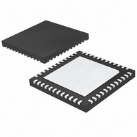
IC ADC 10BIT 105MSPS SAMPL 48QFN
Manufacturer
Linear Technology
Datasheet
1.LTC2232IUKPBF.pdf
(28 pages)
Specifications of LTC2232CUK
Number Of Bits
10
Sampling Rate (per Second)
105M
Data Interface
Parallel
Number Of Converters
1
Power Dissipation (max)
535mW
Voltage Supply Source
Single Supply
Operating Temperature
0°C ~ 70°C
Mounting Type
Surface Mount
Package / Case
48-WFQFN, Exposed Pad
Lead Free Status / RoHS Status
Contains lead / RoHS non-compliant
Available stocks
Company
Part Number
Manufacturer
Quantity
Price
Company:

Part Number:
LTC2232CUK#PBF
Manufacturer:
Linear Technology
Quantity:
135
Part Number:
LTC2232CUK#PBF
Manufacturer:
LINEAR/凌特
Quantity:
20 000


LTC2232/LTC2233
APPLICATIO S I FOR ATIO
Data Format
The LTC2232/LTC2233 parallel digital output can be se-
lected for offset binary or 2’s complement format. The
format is selected with the MODE pin. Connecting MODE
to GND or 1/3V
Connecting MODE to 2/3V
ment output format. An external resistor divider can be
used to set the 1/3V
shows the logic states for the MODE pin.
22
Table 2. MODE Pin Function
MODE Pin
0
1/3V
2/3V
V
Overflow Bit
When OF outputs a logic high the converter is either
overranged or underranged.
Output Clock
The ADC has a delayed version of the ENC
as a digital output, CLKOUT. The CLKOUT pin can be used
to synchronize the converter data to the digital system. This
is necessary when using a sinusoidal encode. Data will be
updated just after CLKOUT rises and can be latched on the
falling edge of CLKOUT.
DD
DD
DD
2’s Complement
2’s Complement
Output Format
DD
Offset Binary
Offset Binary
U
selects offset binary output format.
DD
or 2/3V
U
DD
or V
DD
DD
W
logic values. Table 2
selects 2’s comple-
Cycle Stablizer
Clock Duty
+
Off
Off
On
On
input available
U
Output Driver Power
Separate output power and ground pins allow the output
drivers to be isolated from the analog circuitry. The power
supply for the digital output buffers, OV
to the same power supply as for the logic being driven. For
example if the converter is driving a DSP powered by a 1.8V
supply then OV
OV
can be powered with any voltage from GND up to 1V and
must be less than OV
tween OGND and OV
Output Enable
The outputs may be disabled with the output enable pin, OE.
OE high disables all data outputs including OF and CLKOUT.
The data access and bus relinquish times are too slow to
allow the outputs to be enabled and disabled during full
speed operation. The output Hi-Z state is intended for use
during long periods of inactivity.
Sleep and Nap Modes
The converter may be placed in shutdown or nap modes
to conserve power. Connecting SHDN to GND results in
normal operation. Connecting SHDN to V
results in sleep mode, which powers down all circuitry
including the reference and typically dissipates 1mW. When
exiting sleep mode it will take milliseconds for the output
data to become valid because the reference capacitors have
DD
can be powered with any voltage up to 3.6V. OGND
DD
should be tied to that same 1.8V supply.
DD
DD
.
. The logic outputs will swing be-
DD
DD
, should be tied
and OE to V
22323fa
DD
Related parts for LTC2232CUK
Image
Part Number
Description
Manufacturer
Datasheet
Request
R

Part Number:
Description:
10-Bit,105Msps/80Msps ADCs
Manufacturer:
LINER [Linear Technology]
Datasheet:

Part Number:
Description:
CD ROM LINEARVIEW DATASHEETS
Manufacturer:
Linear Technology

Part Number:
Description:
Standalone Linear Li-Ion Battery Charger with Thermal Regulation in ThinSOT
Manufacturer:
Linear Technology Corporation
Datasheet:
Part Number:
Description:
Low noise, high frequency, 8th order linear phase lowpass filter
Manufacturer:
Linear Technology Corporation
Datasheet:
Part Number:
Description:
Manufacturer:
Linear Technology Corporation
Datasheet:
Part Number:
Description:
Manufacturer:
Linear Technology Corporation
Datasheet:
Part Number:
Description:
Manufacturer:
Linear Technology Corporation
Datasheet:
Part Number:
Description:
Manufacturer:
Linear Technology Corporation
Datasheet:
Part Number:
Description:
Manufacturer:
Linear Technology Corporation
Datasheet:
Part Number:
Description:
Manufacturer:
Linear Technology Corporation
Datasheet:
Part Number:
Description:
Manufacturer:
Linear Technology Corporation
Datasheet:
Part Number:
Description:
Dual and Quad, JFET Input Precision High Speed Op Amps
Manufacturer:
Linear Technology Corporation
Datasheet:
Part Number:
Description:
Manufacturer:
Linear Technology Corporation
Datasheet:
Part Number:
Description:
1, 2, 6 and 8 Channel, 10-Bit Serial I/O Data Acquisition Systems
Manufacturer:
Linear Technology Corporation
Datasheet:
Part Number:
Description:
Manufacturer:
Linear Technology Corporation
Datasheet: