LTC2232CUK Linear Technology, LTC2232CUK Datasheet
LTC2232CUK
Specifications of LTC2232CUK
Available stocks


Related parts for LTC2232CUK


LTC2232CUK Summary of contents
Page 1
... PECL, LVDS, TTL, or CMOS inputs. An optional clock duty cycle stabilizer allows high performance at full speed for a wide range of clock duty cycles. , LTC and LT are registered trademarks of Linear Technology Corporation. All other trademarks are the property of their respective owners. 3. ...
Page 2
... ORDER PART NUMBER LTC2232CUK LTC2232IUK LTC2233CUK LTC2233IUK Order Options Tape and Reel: Add #TR Lead Free: Add #PBF Lead Free Tape and Reel: Add #TRPBF Lead Free Part Marking: *The temperature grade is identified by a label on the shipping container. Consult LTC Marketing for parts specified with wider operating temperature ranges. ...
Page 3
ALOG I PUT The ● denotes the specifications which apply over the full operating temperature range, otherwise specifications are 25°C. (Note 4) A SYMBOL PARAMETER V Analog Input Range ( Analog ...
Page 4
LTC2232/LTC2233 TER AL REFERE CE CHARACTERISTICS PARAMETER V Output Voltage CM V Output Tempco CM V Line Regulation CM V Output Resistance DIGITAL I PUTS A D DIGITAL OUTPUTS full operating temperature range, ...
Page 5
W U POWER REQUIRE E TS range, otherwise specifications are SYMBOL PARAMETER V Analog Supply Voltage DD OV Output Supply Voltage DD I Analog Supply Current VDD P Power Dissipation DISS P Shutdown Power SHDN P Nap ...
Page 6
LTC2232/LTC2233 W U TYPICAL PERFOR A CE CHARACTERISTICS LTC2232: INL, 2V Range 1.0 0.8 0.6 0.4 0.2 0 – 0.2 – 0.4 – 0.6 – 0.8 – 1.0 0 256 512 768 1024 OUTPUT CODE 2232 G01 LTC2232: SNR vs ...
Page 7
TYPICAL PERFOR A CE CHARACTERISTICS LTC2232: SFDR and SNR vs Sample Rate, 1V Range 30MHz, –1dB SFDR SNR SAMPLE RATE (Msps) LTC2232: SFDR vs ...
Page 8
LTC2232/LTC2233 W U TYPICAL PERFOR A CE CHARACTERISTICS LTC2232: 8192 Point FFT 70MHz, –1dB, 1V Range IN 0 –10 –20 –30 –40 –50 –60 –70 –80 –90 –100 –110 –120 ...
Page 9
W U TYPICAL PERFOR A CE CHARACTERISTICS LTC2233: INL, 2V Range 1.0 0.8 0.6 0.4 0.2 0 –0.2 –0.4 –0.6 –0.8 –1.0 0 256 512 768 1024 OUTPUT CODE 2232 G01 LTC2233: SNR vs Input Frequency, –1dB, 1V Range 65 ...
Page 10
LTC2232/LTC2233 W U TYPICAL PERFOR A CE CHARACTERISTICS LTC2233: SFDR and SNR vs Sample Rate, 1V Range 30MHz, –1dB IN 85 SFDR SNR 100 SAMPLE RATE ...
Page 11
W U TYPICAL PERFOR A CE CHARACTERISTICS LTC2233: 8192 Point FFT 70MHz, –1dB, 1V Range IN 0 –10 –20 –30 –40 –50 –60 –70 –80 –90 –100 –110 –120 ...
Page 12
LTC2232/LTC2233 CTIO (Pin 1): Positive Differential Analog Input – (Pin 2): Negative Differential Analog Input. IN REFHA (Pins 3, 4): ADC High Reference. Bypass to Pins 5, 6 with 0.1µF ...
Page 13
U U FUNCTIONAL BLOCK DIAGRA + A IN INPUT FIRST PIPELINED S/H ADC STAGE – 1.6V CM REFERENCE 2.2µF RANGE SELECT REF BUF SENSE DIAGRA S ANALOG INPUT – ENC + ...
Page 14
LTC2232/LTC2233 U U APPLICATIO S I FOR ATIO DYNAMIC PERFORMANCE Signal-to-Noise Plus Distortion Ratio The signal-to-noise plus distortion ratio [S/(N + D)] is the ratio between the RMS amplitude of the fundamental input frequency and the RMS amplitude of all ...
Page 15
U U APPLICATIO S I FOR ATIO CONVERTER OPERATION As shown in Figure 1, the LTC2232/LTC2233 is a CMOS pipelined multistep converter. The converter has five pipelined ADC stages; a sampled analog input will result in a digitized value five ...
Page 16
LTC2232/LTC2233 U U APPLICATIO S I FOR ATIO During the sample phase when ENC is low, the transistors connect the analog inputs to the sampling capacitors and they charge to, and track the differential input voltage. When ENC transitions from ...
Page 17
U U APPLICATIO S I FOR ATIO Figure 4 demonstrates the use of a differential amplifier to convert a single ended input signal into a differential input signal. The advantage of this method is that it provides low frequency input ...
Page 18
LTC2232/LTC2233 U U APPLICATIO S I FOR ATIO HIGH SPEED DIFFERENTIAL 25Ω AMPLIFIER ANALOG + + INPUT CM – – 25Ω AMPLIFIER = LTC6600-20, AD8138, ETC. Figure 4. Differential Drive with an Amplifier 0.1µF 12Ω ANALOG INPUT 0.1µF 25Ω T1 ...
Page 19
U U APPLICATIO S I FOR ATIO 0.1µF 4.7nH ANALOG INPUT 0.1µF 25Ω T1 0.1µF 25Ω 4.7nH T1 = MA/COM ETC1-1-13 RESISTORS, CAPACITORS ARE 0402 PACKAGE SIZE INDUCTORS 0603 OR 0402 Figure 8. Recommended Front End Circuit for Input Frequencies ...
Page 20
LTC2232/LTC2233 U U APPLICATIO S I FOR ATIO Input Range The input range can be set based on the application. The 2V input range will provide the best signal-to-noise perfor- mance while maintaining excellent SFDR. The 1V input range will ...
Page 21
U U APPLICATIO S I FOR ATIO The lower limit of the LTC2232/LTC2233 sample rate is determined by droop of the sample-and-hold circuits. The pipelined architecture of this ADC relies on storing analog signals on small valued capacitors. Junction leakage ...
Page 22
LTC2232/LTC2233 U U APPLICATIO S I FOR ATIO Data Format The LTC2232/LTC2233 parallel digital output can be se- lected for offset binary or 2’s complement format. The format is selected with the MODE pin. Connecting MODE to GND or 1/3V ...
Page 23
U U APPLICATIO S I FOR ATIO to recharge and stabilize. Connecting SHDN GND results in nap mode, which typically dissipates 30mW. In nap mode, the on-chip reference circuit is kept on, so that recovery from nap ...
Page 24
LTC2232/LTC2233 U U APPLICATIO S I FOR ATIO Clock Sources for Undersampling Undersampling raises the bar on the clock source and the higher the input frequency, the greater the sensitivity to clock jitter or phase noise. A clock source that ...
Page 25
U U APPLICATIO S I FOR ATIO R19 R1* C1 OPT 0.1µF T1* R2 ANALOG 24.9 INPUT J1 C2* R4 24.9 C3 0.1µF R6 0.1µ 1µF 0.1µF ...
Page 26
LTC2232/LTC2233 U U APPLICATIO S I FOR ATIO Layer 1 Component Side Layer 3 Power Plane Silkscreen Top Layer 2 GND Plane Layer 4 Bottom Side 22323fa ...
Page 27
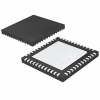
... SHADED AREA IS ONLY A REFERENCE FOR PIN 1 LOCATION ON THE TOP AND BOTTOM OF PACKAGE Information furnished by Linear Technology Corporation is believed to be accurate and reliable. However, no responsibility is assumed for its use. Linear Technology Corporation makes no represen- tation that the interconnection of its circuits as described herein will not infringe on existing patent rights. ...
Page 28
... Integrated LO Quadrature Generator High IIP3: 21.5dBm at 900MHz, Integrated LO Quadrature Generator High IIP3: 21dBm at 800MHz, Integrated LO Quadrature Generator 4.5V to 5.25V Supply, 25dBm IIP3 at 900MHz 12.5dB, 50Ω Single-Ended RF and LO Ports www.linear.com ● 22323fa LT 0106 REV A • PRINTED IN USA © LINEAR TECHNOLOGY CORPORATION 2004 ...