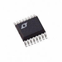
LTC1402CGN Linear Technology, LTC1402CGN Datasheet - Page 2

LTC1402CGN
Manufacturer Part Number
LTC1402CGN
Description
IC ADC 12BIT 2.2MSPS SHDN 16SSOP
Manufacturer
Linear Technology
Datasheet
1.LTC1402CGNPBF.pdf
(24 pages)
Specifications of LTC1402CGN
Number Of Bits
12
Sampling Rate (per Second)
2.2M
Data Interface
MICROWIRE™, Serial, SPI™
Number Of Converters
1
Power Dissipation (max)
150mW
Voltage Supply Source
Analog and Digital, Dual ±
Operating Temperature
0°C ~ 70°C
Mounting Type
Surface Mount
Package / Case
16-SSOP (0.150", 3.90mm Width)
Lead Free Status / RoHS Status
Contains lead / RoHS non-compliant
Available stocks
Company
Part Number
Manufacturer
Quantity
Price
Company:
Part Number:
LTC1402CGN
Manufacturer:
LT
Quantity:
10 000
Part Number:
LTC1402CGN#TRPBF
Manufacturer:
LINEAR/凌特
Quantity:
20 000
ABSOLUTE
CONVERTER CHARACTERISTICS
A ALOG I PUT
LTC1402
AV
Supply Voltage (V
Negative Supply Voltage (V
Total Supply Voltage (V
Analog Input Voltage
Digital Input Voltage
Digital Output Voltage ......... (V
Power Dissipation .............................................. 250mW
Operation Temperature Range
Storage Temperature Range ................. – 65 C to 150 C
Lead Temperature (Soldering, 10 sec).................. 300 C
temperature range, otherwise specifications are at T
PARAMETER
Resolution (No Missing Codes)
Integral Linearity Error
Differential Linearity
Offset Error
Full-Scale Error
Full-Scale Tempco
otherwise specifications are at T
SYMBOL
V
V
I
C
t
t
t
CMRR
2
IN
ACQ
AP
JITTER
IN
CM
IN
U
DD
(Note 3) .......................... (V
(Note 4) .......................... (V
LTC1402C ............................................... 0 C to 70 C
LTC1402I ............................................ – 40 C to 85 C
U
= DV
DD
PARAMETER
Analog Differential Input Range (Notes 3, 11)
Analog Common Mode + Differential
Input Range (Note 12)
Analog Input Leakage Current
Analog Input Capacitance
Sample-and-Hold Acquisition Time
Sample-and-Hold Aperture Delay Time
Sample-and-Hold Aperture Delay Time Jitter
Analog Input Common Mode Rejection Ratio
= OV
DD
U
DD
W
MAXIMUM
= V
) ................................................. 6V
DD
(Notes 1, 2)
DD
The
to V
W W
SS
A
) ............................... – 6V
= 25 C. (Note 5)
SS
SS
SS
SS
denotes the specifications which apply over the full operating temperature range,
) .......................... 12V
– 0.3V) to (V
– 0.3V) to (V
– 0.3V) to (V
RATINGS
U
A
DD
DD
DD
= 25 C. With internal reference (Note 5).
CONDITIONS
(Note 6)
(Note 6)
(Note 6)
(Note 6)
Internal Reference (Note 6)
External Reference
CONDITIONS
Bipolar Mode with BIP/UNI High
Unipolar Mode with BIP/UNI Low
Dual 5V Supply
Single 5V Supply
(Note 9)
f
f
IN
IN
+ 0.3V)
+ 0.3V)
+ 0.3V)
4.75V V
4.75V V
– 5.25V V
– 5.25V V
= 1MHz, V
= 100MHz, V
The
DD
DD
denotes the specifications which apply over the full operating
SS
SS
IN
= 2V to – 2V
PACKAGE/ORDER
IN
5.25V
Consult factory for Military grade parts.
5.25V
–4.75V
0V
= 2V to – 2V
BIP/UNI
AGND1
AGND2
AV
GAIN
V
A
A
16-LEAD NARROW PLASTIC SSOP
REF
IN
IN
DD
T
+
–
JMAX
1
2
3
4
5
6
7
8
= 125 C,
GN PACKAGE
TOP VIEW
JA
= 150 C/ W
16
15
14
13
12
11
10
9
CONV
SCK
V SS
DGND
DV
0V
D
OGND
MIN
MIN
OUT
12
DD
DD
INFORMATION
U
0 to 4.096
–2.5 to 5
0 to 5
TYP
TYP
2.048
– 62
– 24
GN PART MARKING
0.35
0.25
2.6
10
10
15
1
2
1
ORDER PART
LTC1402CGN
LTC1402IGN
NUMBER
W
1402
1402I
MAX
MAX
57
10
15
1
1
1
ppm/ C
ppm/ C
UNITS
UNITS
U
LSB
LSB
LSB
LSB
Bits
dB
dB
pF
ns
ns
ps
V
V
V
V
A


