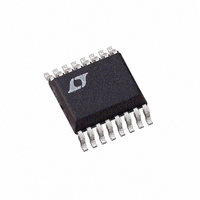
LTC2413IGN#TR Linear Technology, LTC2413IGN#TR Datasheet - Page 29

LTC2413IGN#TR
Manufacturer Part Number
LTC2413IGN#TR
Description
IC ADC 24BIT 50/60HZ MPWR 16SSOP
Manufacturer
Linear Technology
Datasheet
1.LTC2413CGN.pdf
(44 pages)
Specifications of LTC2413IGN#TR
Number Of Bits
24
Sampling Rate (per Second)
6.8
Data Interface
MICROWIRE™, Serial, SPI™
Number Of Converters
2
Power Dissipation (max)
1mW
Voltage Supply Source
Single Supply
Operating Temperature
-40°C ~ 85°C
Mounting Type
Surface Mount
Package / Case
16-SSOP (0.150", 3.90mm Width)
Lead Free Status / RoHS Status
Contains lead / RoHS non-compliant
Available stocks
Company
Part Number
Manufacturer
Quantity
Price
APPLICATIO S I FOR ATIO
Output Data Rate
When using its internal oscillator, the LTC2413 can pro-
duce up to 6.8 readings per second. The actual output data
rate will depend upon the length of the sleep and data
output phases which are controlled by the user and which
can be made insignificantly short. When operated with an
external conversion clock (F
oscillator), the LTC2413 output data rate can be increased
as desired. The duration of the conversion phase is 20510/
f
internal oscillator is used with simultaneous 50Hz/60Hz
rejection. There is no significant difference in the LTC2413
performance between these two operation modes.
An increase in f
translate into a proportional increase in the maximum
output data rate. This substantial advantage is neverthe-
less accompanied by three potential effects, which must
be carefully considered.
EOSC
. If f
EOSC
= 139800Hz, the converter behaves as if the
EOSC
U
over the nominal 139800Hz will
U
O
Figure 27. INL vs Differential Input Voltage (V
and Reference Source Resistance (R
Large C
connected to an external
W
REF
Values (C
–12
–15
15
12
–3
–6
–9
9
6
3
0
–0.5 –0.4–0.3–0.2–0.1 0 0.1 0.2 0.3 0.4 0.5
V
REF+ = 5V
REF– = GND
V
U
CC
INCM
R
= 5V
REF
SOURCE
= 0.5 • (IN
1 F)
= 100
R
SOURCE
V
+
INDIF
+ IN
/V
R
= 1000
–
First, a change in f
in the internal notch position and in a reduction of the
converter differential mode rejection at the power-line
frequency. In many applications, the subsequent perfor-
mance degradation can be substantially reduced by rely-
ing upon the LTC2413’s exceptional common mode rejec-
tion and by carefully eliminating common mode to differ-
ential mode conversion sources in the input circuit. The
user should avoid single-ended input filters and should
maintain a very high degree of matching and symmetry in
the circuits driving the IN
Second, the increase in clock frequency will increase
proportionally the amount of sampling charge transferred
through the input and the reference pins. If large external
input and/or reference capacitors (C
previous section provides formulae for evaluating the
effect of the source resistance upon the converter perfor-
mance for any value of f
or reference capacitors (C
the external source resistance upon the LTC2413 typical
performance can be inferred from Figures 18, 19, 23 and
24 in which the horizontal axis is scaled by 139800/f
SOURCE
) = 2.5V
REFDIF
SOURCE
= 500
F
C
T
O
A
REF
at REF
= GND
= 25 C
IN
= 10 F
2413 F27
= IN
+
and REF
+
– IN
EOSC
–
)
–
will result in a proportional change
for
EOSC
+
IN
and IN
, C
. If small external input and/
REF
) are used, the effect of
–
IN
pins.
, C
LTC2413
REF
) are used, the
sn2413 2413fs
29
EOSC
.


