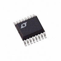
LTC2413IGN#TR Linear Technology, LTC2413IGN#TR Datasheet - Page 12

LTC2413IGN#TR
Manufacturer Part Number
LTC2413IGN#TR
Description
IC ADC 24BIT 50/60HZ MPWR 16SSOP
Manufacturer
Linear Technology
Datasheet
1.LTC2413CGN.pdf
(44 pages)
Specifications of LTC2413IGN#TR
Number Of Bits
24
Sampling Rate (per Second)
6.8
Data Interface
MICROWIRE™, Serial, SPI™
Number Of Converters
2
Power Dissipation (max)
1mW
Voltage Supply Source
Single Supply
Operating Temperature
-40°C ~ 85°C
Mounting Type
Surface Mount
Package / Case
16-SSOP (0.150", 3.90mm Width)
Lead Free Status / RoHS Status
Contains lead / RoHS non-compliant
Available stocks
Company
Part Number
Manufacturer
Quantity
Price
APPLICATIO S I FOR ATIO
LTC2413
Once CS is pulled LOW, the device begins outputting the
conversion result. There is no latency in the conversion
result. The data output corresponds to the conversion just
performed. This result is shifted out on the serial data out
pin (SDO) under the control of the serial clock (SCK). Data
is updated on the falling edge of SCK allowing the user to
reliably latch data on the rising edge of SCK (see Figure 3).
The data output state is concluded once 32 bits are read
out of the ADC or when CS is brought HIGH. The device
automatically initiates a new conversion and the cycle
repeats.
Through timing control of the CS and SCK pins, the
LTC2413 offers several flexible modes of operation
(internal or external SCK and free-running conversion
modes). These various modes do not require program-
ming configuration registers; moreover, they do not dis-
turb the cyclic operation described above. These modes of
operation are described in detail in the Serial Interface
Timing Modes section.
Conversion Clock
A major advantage the delta-sigma converter offers over
conventional type converters is an on-chip digital filter
(commonly implemented as a sinc or comb filter). For high
resolution, low frequency applications, this filter is de-
signed to simultaneously reject line frequencies of 50Hz
and 60Hz plus their harmonics. The filter rejection perfor-
mance is directly related to the accuracy of the converter
system clock. The LTC2413 incorporates a highly accu-
rate on-chip oscillator. This eliminates the need for exter-
nal frequency setting components such as crystals or
oscillators. The LTC2413 achieves a minimum of 87dB
over the range of 49Hz to 61.2Hz.
Ease of Use
The LTC2413 data output has no latency, filter settling
delay or redundant data associated with the conversion
cycle. There is a one-to-one correspondence between the
conversion and the output data. Therefore, multiplexing
multiple analog voltages is easy.
12
U
U
W
U
The LTC2413 performs offset and full-scale calibrations in
every conversion cycle. This calibration is transparent to
the user and has no effect on the cyclic operation de-
scribed above. The advantage of continuous calibration is
extreme stability of offset and full-scale readings with re-
spect to time, supply voltage change and temperature drift.
Power-Up Sequence
The LTC2413 automatically enters an internal reset state
when the power supply voltage V
mately 2.2V. This feature guarantees the integrity of the
conversion result and of the serial interface mode selec-
tion. (See the 2-wire I/O sections in the Serial Interface
Timing Modes section.)
When the V
the converter creates an internal power-on-reset (POR)
signal with a duration of approximately 0.5ms. The POR
signal clears all internal registers. Following the POR
signal, the LTC2413 starts a normal conversion cycle and
follows the succession of states described above. The first
conversion result following POR is accurate within the
specifications of the device if the power supply voltage is
restored within the operating range (2.7V to 5.5V) before
the end of the POR time interval.
Reference Voltage Range
This converter accepts a truly differential external refer-
ence voltage. The absolute/common mode voltage speci-
fication for the REF
from GND to V
REF
The LTC2413 can accept a differential reference voltage
from 0.1V to V
mined by the thermal noise of the front-end circuits, and
as such, its value in nanovolts is nearly constant with
reference voltage. A decrease in reference voltage will not
significantly improve the converter’s effective resolution.
On the other hand, a reduced reference voltage will im-
prove the converter’s overall INL performance. A reduced
reference voltage will also improve the converter perfor-
mance when operated with an external conversion clock
(external F
rates (see the Output Data Rate section).
+
pin must always be more positive than the REF
O
CC
signal) at substantially higher output data
voltage rises above this critical threshold,
CC
CC
. The converter output noise is deter-
. For correct converter operation, the
+
and REF
–
pins covers the entire range
CC
drops below approxi-
sn2413 2413fs
–
pin.


