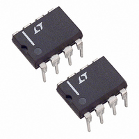
LTC1288CN8 Linear Technology, LTC1288CN8 Datasheet

LTC1288CN8
Specifications of LTC1288CN8
Available stocks
Related parts for LTC1288CN8
LTC1288CN8 Summary of contents
Page 1
... The high impedance analog inputs and the ability to operate with reduced spans (to 1.5V full scale) allow direct connection to sensors and transducers in many applications, eliminating the need for gain stages. , LTC and LT are registered trademarks of Linear Technology Corporation MPU (e.g., 8051) P1 ...
Page 2
... Lead Temperature (Soldering, 10 sec.)................ 300 ORDER PART NUMBER V 1 REF +IN 2 LTC1285CN8 –IN 3 GND 4 8-LEAD PLASTIC 150 C, JMAX ORDER PART NUMBER CS/SHDN 1 CH0 2 LTC1288CN8 CH1 3 GND 4 8-LEAD PLASTIC SO T JMAX CONDITIONS LTC1285 LTC1288 V = 2.7V CC LTC1285, f CLK LTC1288, f CLK V = 2.7V CC LTC1285 LTC1288, V ...
Page 3
CONVERTER AND MULTIPLEXER CHARACTERISTICS PARAMETER Resolution (No Missing Codes) Integral Linearity Error Differential Linearity Error Offset Error Gain Error Analog Input Range REF Input Range (LTC1285) (Notes 7, 8, and 9) Analog Input Leakage Current (Note 10) ...
Page 4
LTC1285/LTC1288 AC CHARACTERISTICS SYMBOL PARAMETER t Analog Input Sample Time SMPL f Maximum Sampling Frequency SMPL (MAX) t Conversion Time CONV t Delay Time, CLK to D Data Valid dDO OUT t Delay Time Hi-Z dis OUT ...
Page 5
W U TYPICAL PERFORMANCE CHARACTERISTICS Reference Current vs Sample Rate (LTC1285 25° 2. 2.5V REF 120kHz CLK ...
Page 6
LTC1285/LTC1288 W TYPICAL PERFORMANCE CHARACTERISTICS Spurious-Free Dynamic Range vs Input Frequency 100 25° 2. 2.5V REF SMPL SMPL(MAX ...
Page 7
W TYPICAL PERFORMANCE CHARACTERISTICS Minimum Clock Frequency for 0.1 LSB Error vs Temperature 120 2.5V REF 100 TEMPERATURE (°C) LTC1285/88 • ...
Page 8
LTC1285/LTC1288 W BLOCK DIAGRAM + IN (CH0) – IN (CH1) PIN NAMES IN PARENTHESES REFER TO THE LTC1288 TEST CIRCUITS Load Circuit for dDO 1. OUT 100pF Voltage Waveforms for D Delay Times, t OUT ...
Page 9
TEST CIRCUITS Voltage Waveforms for OUT WAVEFORM 1 (SEE NOTE 1) D OUT WAVEFORM 2 (SEE NOTE 2) NOTE 1: WAVEFORM 1 IS FOR AN OUTPUT WITH INTERNAL CONDITIONS SUCH THAT THE OUTPUT IS HIGH UNLESS DISABLED ...
Page 10
LTC1285/LTC1288 U U APPLICATION INFORMATION OVERVIEW The LTC1285 and LTC1288 are 3V micropower, 12-bit, successive approximation sampling A/D converters. The LTC1285 typically draws 160 A of supply current when sampling at 7.5kHz while the LTC1288 nominally con- sumes 210 A ...
Page 11
U U APPLICATION INFORMATION MSB-First Data (MSBF = suCS CLK ODD/ START SIGN D IN SGL/ MSBF DIFF NULL HI-Z BIT D OUT B11 B10 B9 t (MSB) SMPL MSB-First Data (MSBF = suCS ...
Page 12
LTC1285/LTC1288 U U APPLICATION INFORMATION Data Transfer The CLK synchronizes the data transfer with each bit being transmitted on the falling CLK edge and captured on the rising CLK edge in both transmitting and receiving systems. The LTC1285 does not ...
Page 13
U U APPLICATION INFORMATION Transfer Curve The LTC1285/LTC1288 are permanently configured for unipolar only. The input span and code assignment for this conversion type are shown in the following figures. Transfer Curve ...
Page 14
LTC1285/LTC1288 U U APPLICATION INFORMATION Several things must be taken into account to achieve such a low power consumption. Shutdown The LTC1285/LTC1288 are equipped with automatic shut- down features. They draw power when the CS pin is low and shut ...
Page 15
U U APPLICATION INFORMATION of Maximum Clock Rate vs Supply Voltage). If the maxi- mum clock frequency is used, care must be taken to ensure that the device converts correctly. Mixed Supplies It is possible to have a microprocessor running ...
Page 16
LTC1285/LTC1288 U U APPLICATION INFORMATION Single-Ended Inputs The sample-and-hold of the LTC1288 allows conversion of rapidly varying signals. The input voltage is sampled during the t time as shown in Figure 7. The sampling SMPL interval begins as the bit ...
Page 17
U U APPLICATION INFORMATION selected “+” and “–” inputs once during each conversion cycle. Large external source resistors and capacitances will slow the settling of the inputs important that the overall RC time constants be short enough to ...
Page 18
LTC1285/LTC1288 U U APPLICATION INFORMATION Voltage). However, care must be taken when operating at low values of V because of the reduced LSB step size REF and the resulting higher accuracy requirement placed on the converter. The following factors must ...
Page 19
U U APPLICATION INFORMATION Signal-to-Noise Ratio The Signal-to-Noise plus Distortion Ratio (S the ratio between the RMS amplitude of the fundamental input frequency to the RMS amplitude of all other fre- quency components at the ADC’s output. ...
Page 20
LTC1285/LTC1288 TYPICAL APPLICATIONS MICROPROCESSOR INTERFACES The LTC1285/LTC1288 can interface directly without ex- ternal hardware to most popular microprocessor (MPU) synchronous serial formats (see Table 1 MPU without a dedicated serial port is used, then ...
Page 21
TYPICAL APPLICATIONS CS CLK OUT MPU TRANSMIT WORD BYTE 1 MPU RECEIVED ? ? ? ? ? ? ? WORD BYTE 1 D OUT FROM LTC1298 STORED IN MC68HC11 RAM ...
Page 22
LTC1285/LTC1288 TYPICAL APPLICATIONS Interfacing to the Parallel Port of the INTEL 8051 Family The Intel 8051 has been chosen to demonstrate the interface between the LTC1288 and parallel port micro- processors. Normally the CS, CLK and D be generated on ...
Page 23
... Figure 14. Scope Trace the LTC1285 “Quick Look” Circuit Showing A/D Output 101010101010 (AAA Information furnished by Linear Technology Corporation is believed to be accurate and reliable. However, no responsibility is assumed for its use. Linear Technology Corporation makes no represen- tation that the interconnection of its circuits as described herein will not infringe on existing patent rights. U ...
Page 24
... MAX 0.255 0.015* (6.477 0.381) 0.015 (0.380 MIN 0.189 – 0.197* (4.801 – 5.004 0.150 – 0.157** 0.228 – 0.244 (3.810 – 3.988) (5.791 – 6.197 LT/GP 0894 10K • PRINTED IN USA LINEAR TECHNOLOGY CORPORATION 1994 0695 SO8 0695 ...


