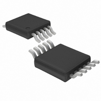
LTC2411-1CMS#TR Linear Technology, LTC2411-1CMS#TR Datasheet - Page 17

LTC2411-1CMS#TR
Manufacturer Part Number
LTC2411-1CMS#TR
Description
IC A/DCONV DIFF INPUT&REF 10MSOP
Manufacturer
Linear Technology
Datasheet
1.LTC2411CMSPBF.pdf
(40 pages)
Specifications of LTC2411-1CMS#TR
Number Of Bits
24
Sampling Rate (per Second)
6.8
Data Interface
MICROWIRE™, Serial, SPI™
Number Of Converters
2
Power Dissipation (max)
1mW
Voltage Supply Source
Single Supply
Operating Temperature
0°C ~ 70°C
Mounting Type
Surface Mount
Package / Case
10-TFSOP, 10-MSOP (0.118", 3.00mm Width)
Lead Free Status / RoHS Status
Contains lead / RoHS non-compliant
Other names
LTC2411-1CMSTR
LTC24111CMSTR
LTC24111CMSTR
Available stocks
Company
Part Number
Manufacturer
Quantity
Price
APPLICATIO S I FOR ATIO
device automatically enters the low power sleep state once
the conversion is complete.
When the device is in the sleep state (EOC = 0), its
conversion result is held in an internal static shift regis-
ter. The device remains in the sleep state until the first
rising edge of SCK is seen while CS is LOW. Data is shifted
out the SDO pin on each falling edge of SCK. This enables
external circuitry to latch the output on the rising edge of
SCK. EOC can be latched on the first rising edge of SCK
and the last bit of the conversion result can be latched on
the 32nd rising edge of SCK. On the 32nd falling edge of
SCK, the device begins a new conversion. SDO goes HIGH
(EOC = 1) indicating a conversion is in progress.
At the conclusion of the data cycle, CS may remain LOW
and EOC monitored as an end-of-conversion interrupt.
Alternatively, CS may be driven HIGH setting SDO to Hi-Z.
As described above, CS may be pulled LOW at any time in
order to monitor the conversion status.
Typically, CS remains LOW during the data output state.
However, the data output state may be aborted by pulling
CS HIGH anytime between the first rising edge and the 32nd
falling edge of SCK, see Figure 6. On the rising edge of CS,
the device aborts the data output state and immediately
initiates a new conversion. This is useful for systems not
(EXTERNAL)
SDO
SCK
CS
SLEEP
BIT 0
EOC
U
CONVERSION
Hi-Z
U
DATA OUTPUT
TEST EOC
Hi-Z
Figure 6. External Serial Clock, Reduced Data Output Length
TEST EOC
W
ANALOG INPUT RANGE
SLEEP
–0.5V
Hi-Z
REF
0.1V TO V
REFERENCE
BIT 31
TO 0.5V
EOC
VOLTAGE
U
1 F
2.7V TO 5.5V
REF
CC
BIT 30
1
2
3
4
5
6
V
REF
REF
IN
IN
GND
CC
LTC2411-1
+
–
LTC2411/
+
–
BIT 29
SDO
SIG
SCK
requiring all 32 bits of output data, aborting an invalid
conversion cycle or synchronizing the start of a conversion.
External Serial Clock, 2-Wire I/O
This timing mode utilizes a 2-wire serial I/O interface. The
conversion result is shifted out of the device by an exter-
nally generated serial clock (SCK) signal, see Figure 7. CS
may be permanently tied to ground, simplifying the user
interface or isolation barrier.
The external serial clock mode is selected at the end of the
power-on reset (POR) cycle. The POR cycle is concluded
approximately 1ms after V
applied to SCK at this time determines if SCK is internal or
external. SCK must be driven LOW prior to the end of POR
in order to enter the external serial clock timing mode.
Since CS is tied LOW, the end-of-conversion (EOC) can be
continuously monitored at the SDO pin during the convert
and sleep states. EOC may be used as an interrupt to an
external controller indicating the conversion result is
ready. EOC = 1 while the conversion is in progress and
EOC = 0 once the conversion enters the low power sleep
state. On the falling edge of EOC, the conversion result is
loaded into an internal static shift register. The device
remains in the sleep state until the first rising edge of SCK.
CS
F
O
10
9
8
7
DATA OUTPUT
BIT 28
MSB
3-WIRE
SPI INTERFACE
V
CC
= 50Hz REJECTION (LTC2411)
= EXTERNAL OSCILLATOR
= 60Hz REJECTION (LTC2411)
= SIMULTANEOUS 50Hz/60Hz REJECTION (LTC2411-1)
BIT 27
LTC2411/LTC2411-1
BIT 9
BIT 8
CC
exceeds 1.9V. The level
CONVERSION
Hi-Z
TEST EOC
2411 F06
17


