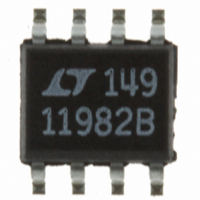
LTC1198-2BCS8 Linear Technology, LTC1198-2BCS8 Datasheet - Page 20

LTC1198-2BCS8
Manufacturer Part Number
LTC1198-2BCS8
Description
IC ADC 8BIT 750KHZ SAMPL 8-SOIC
Manufacturer
Linear Technology
Datasheet
1.LTC1196-2BCS8PBF.pdf
(28 pages)
Specifications of LTC1198-2BCS8
Number Of Bits
8
Sampling Rate (per Second)
750k
Data Interface
Serial
Number Of Converters
1
Power Dissipation (max)
50mW
Voltage Supply Source
Single Supply
Operating Temperature
0°C ~ 70°C
Mounting Type
Surface Mount
Package / Case
8-SOIC (0.154", 3.90mm Width)
Lead Free Status / RoHS Status
Contains lead / RoHS non-compliant
Available stocks
Company
Part Number
Manufacturer
Quantity
Price
Company:
Part Number:
LTC1198-2BCS8
Manufacturer:
LT
Quantity:
10 000
Part Number:
LTC1198-2BCS8
Manufacturer:
LTC
Quantity:
20 000
Part Number:
LTC1198-2BCS8#PBF
Manufacturer:
LINEAR/凌特
Quantity:
20 000
LTC1196/LTC1198
APPLICATIONS INFORMATION
Source Resistance
The analog inputs of the LTC1196/LTC1198 look like
a 25pF capacitor (C
(R
the selected “+” and “–” inputs once during each con-
version cycle. Large external source resistors will slow
the settling of the inputs. It is important that the overall
RC time constants be short enough to allow the analog
inputs to completely settle within t
REFERENCE INPUT
The voltage on the reference input of the LTC1196 defi nes
the voltage span of the A/D converter. The reference
input has transient capacitive switching currents which
are due to the switched-capacitor conversion technique
(see Figure 9). During each bit test of the conversion
(every CLK cycle), a capacitive current spike will be
generated on the reference pin by the ADC. These high
frequency current spikes will settle quickly and do not
cause a problem if the reference input is bypassed with
at least a 0.1μF capacitor.
The reference input can be driven with standard volt-
age references. Bypassing the reference with a 0.1μF
capacitor is recommended to keep the high frequency
impedance low as described above. Some references
require a small resistor in series with the bypass capaci-
tor for frequency stability. See the individual reference
data sheet for details.
20
ON
V
) as shown in Figure 8. C
V
IN
IN
+
–
R
R
Figure 8. Analog Input Equivalent Circuit
SOURCE
SOURCE
+
–
INPUT
INPUT
IN
–
+
) in series with a 120Ω resistor
IN
t
SMPL
t
SMPL
gets switched between
SMPL
120Ω
R
ON
.
LTC1196
LTC1198
C
25pF
1196/98 F08
IN
Reduced Reference Operation
The minimum reference voltage of the LTC1198 is limited
to 2.7V because the V
tied together. However, the LTC1196 can operate with
reference voltages below 1V.
The effective resolution of the LTC1196 can be increased
by reducing the input span of the converter. The LTC1196
exhibits good linearity and gain over a wide range of
reference voltages (see the Linearity and Full-Scale Error
vs Reference Voltage curves in the Typical Performance
Characteristics section). However, care must be taken when
operating at low values of V
LSB step size and the resulting higher accuracy require-
ment placed on the converter. The following factors must
be considered when operating at low V
Offset with Reduced V
The offset of the LTC1196 has a larger effect on the output
code when the ADC is operated with reduced reference
voltage. The offset (which is typically a fi xed voltage) be-
comes a larger fraction of an LSB as the size of the LSB is
reduced. The Unadjusted Offset Error vs Reference Voltage
curve in the Typical Performance Characteristics section
depicts how offset in LSBs is related to reference voltage
for a typical value of V
is 0.1LSB with a 5V reference becomes 0.5LSB with a 1V
reference and 2.5LSB with a 0.2V reference. If this offset is
unacceptable, it can be corrected digitally by the receiving
system or by offsetting the “–” input of the LTC1196.
1. Offset
2. Noise
Figure 9. Reference Input Equivalent Circuit
R
V
OUT
REF
REF
GND
5
4
+
CC
OS
REF
supply and reference are internally
. For example, a V
REF
EVERY CLK CYCLE
because of the reduced
R
ON
REF
OS
LTC1196
values.
of 2mV which
5pF TO
30pF
1196/98 F09
119698fb


