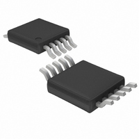
LTC2422CMS#TRPBF Linear Technology, LTC2422CMS#TRPBF Datasheet - Page 20

LTC2422CMS#TRPBF
Manufacturer Part Number
LTC2422CMS#TRPBF
Description
IC ADC 2CH 20BIT MICRPWR 10-MSOP
Manufacturer
Linear Technology
Datasheet
1.LTC2422CMSPBF.pdf
(32 pages)
Specifications of LTC2422CMS#TRPBF
Number Of Bits
20
Sampling Rate (per Second)
7.5
Data Interface
MICROWIRE™, Serial, SPI™
Number Of Converters
2
Power Dissipation (max)
1mW
Voltage Supply Source
Single Supply
Operating Temperature
0°C ~ 70°C
Mounting Type
Surface Mount
Package / Case
10-TFSOP, 10-MSOP (0.118", 3.00mm Width)
Lead Free Status / RoHS Status
Lead free / RoHS Compliant
Available stocks
Company
Part Number
Manufacturer
Quantity
Price
APPLICATIO S I FOR ATIO
LTC2421/LTC2422
Internal Serial Clock, Autostart Conversion
This timing mode is identical to the internal serial clock,
2-wire I/O described above with one additional feature.
Instead of grounding CS, an external timing capacitor is
tied to CS.
While the conversion is in progress, the CS pin is held
HIGH by an internal weak pull-up. Once the conversion is
complete, the device enters the low power sleep state and
an internal 25nA current source begins discharging the
capacitor tied to CS, see Figure 12. The time the converter
spends in the sleep state is determined by the value of the
external timing capacitor, see Figures 13 and 14. Once the
voltage at CS falls below an internal threshold ( 1.4V), the
device automatically begins outputting data. The data out-
put cycle begins on the first rising edge of SCK and ends
on the 24th rising edge. Data is shifted out the SDO pin on
each falling edge of SCK. The internally generated serial
clock is output to the SCK pin. This signal may be used to
shift the conversion result into external circuitry. After the
24th rising edge, CS is pulled HIGH and a new conversion
is immediately started. This is useful in applications re-
quiring periodic monitoring and ultralow power. Figure 15
shows the average supply current as a function of capaci-
tance on CS.
20
(INTERNAL)
SDO
SCK
CS
CONVERSION
U
U
BIT 23
EOC
SLEEP
CH0/CH1
BIT 22
W
Figure 11. Internal Serial Clock, Continuous Operation
ANALOG INPUT RANGE
(V
ZS
REF
REFERENCE VOLTAGE
0V TO FS
BIT 21
ZS
SET
SIG
FS
= FS
SET
SET
– 0.12V
SET
+ 0.1V TO V
U
+ 0.12V
SET
– ZS
– 100mV
BIT 20
REF
EXR
SET
1 F
2.7V TO 5.5V
REF
TO
)
CC
BIT 19
MSB
1
2
3
4
5
V
FS
CH1
ZS
CH0
CC
SET
SET
It should be noticed that the external capacitor discharge
current is kept very small in order to decrease the con-
verter power dissipation in the sleep state. In the autostart
mode, the analog voltage on the CS pin cannot be
observed without disturbing the converter operation
using a regular oscilloscope probe. When using this con-
figuration, it is important to minimize the external leakage
current at the CS pin by using a low leakage external ca-
pacitor and properly cleaning the PCB surface.
The internal serial clock mode is selected every time the
voltage on the CS pin crosses an internal threshold volt-
age. An internal weak pull-up at the SCK pin is active while
CS is discharging; therefore, the internal serial clock tim-
ing mode is automatically selected if SCK is floating. It is
important to ensure there are no external drivers pulling
SCK LOW while CS is discharging.
DIGITAL SIGNAL LEVELS
The LTC2421/LTC2422’s digital interface is easy to use.
Its digital inputs (F
operation) accept standard TTL/CMOS logic levels and the
internal hysteresis receivers can tolerate edge rates as
slow as 100 s. However, some considerations are required
LTC2422
DATA OUTPUT
BIT 18
GND
SDO
SCK
CS
F
O
10
9
8
7
6
V
CC
= INTERNAL OSC/50Hz REJECTION
= EXTERNAL CLOCK SOURCE
= INTERNAL OSC/60Hz REJECTION
O
, CS and SCK in External SCK mode of
BIT 4
LSB
BIT 0
20
V
CC
10k
CONVERSION
24212f
24212 F11


