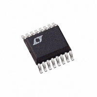
LTC2436-1IGN Linear Technology, LTC2436-1IGN Datasheet - Page 9

LTC2436-1IGN
Manufacturer Part Number
LTC2436-1IGN
Description
IC CONV A/D 16B 2CH DIFF 16SSOP
Manufacturer
Linear Technology
Datasheet
1.LTC2436-1CGN.pdf
(28 pages)
Specifications of LTC2436-1IGN
Number Of Bits
16
Sampling Rate (per Second)
6.8
Data Interface
MICROWIRE™, Serial, SPI™
Number Of Converters
1
Power Dissipation (max)
1mW
Voltage Supply Source
Single Supply
Operating Temperature
-40°C ~ 85°C
Mounting Type
Surface Mount
Package / Case
16-SSOP (0.150", 3.90mm Width)
Lead Free Status / RoHS Status
Contains lead / RoHS non-compliant
Available stocks
Company
Part Number
Manufacturer
Quantity
Price
Company:
Part Number:
LTC2436-1IGN
Manufacturer:
LT
Quantity:
10 000
Part Number:
LTC2436-1IGN#TRPBF
Manufacturer:
LINEAR/凌特
Quantity:
20 000
APPLICATIO S I FOR ATIO
cycle. There is a one-to-one correspondence between the
conversion and the output data. Therefore, multiplexing
multiple analog voltages is easy.
The LTC2436-1 performs offset and full-scale calibrations
every conversion cycle. This calibration is transparent to
the user and has no effect on the cyclic operation de-
scribed above. The advantage of continuous calibration is
extreme stability of offset and full-scale readings with re-
spect to time, supply voltage change and temperature drift.
Power-Up Sequence
The LTC2436-1 automatically enters an internal reset state
when the power supply voltage V
mately 2V. This feature guarantees the integrity of the
conversion result and of the serial interface mode selec-
tion. (See the 2-wire I/O sections in the Serial Interface
Timing Modes section.)
When the V
the converter creates an internal power-on-reset (POR)
signal with a typical duration of 1ms. The POR signal clears
all internal registers and selects channel 0. Following the
POR signal, the LTC2436-1 starts a normal conversion
cycle and follows the succession of states described above.
The first conversion result following POR is accurate within
the specifications of the device if the power supply voltage
is restored within the operating range (2.7V to 5.5V) be-
fore the end of the POR time interval.
Reference Voltage Range
This converter accepts a truly differential external refer-
ence voltage. The absolute/common mode voltage speci-
fication for the REF
from GND to V
REF
The LTC2436-1 can accept a differential reference voltage
from 0.1V to V
mined by the thermal noise of the front-end circuits, and
as such, its value in nanovolts is nearly constant with
reference voltage. A decrease in reference voltage will
significantly improve the converter’s effective resolution,
since the thermal noise (800nV) is well below the quanti-
zation level of the device (75.6 V for a 5V reference). At the
minimum reference (100mV) the thermal noise
+
pin must always be more positive than the REF
CC
voltage rises above this critical threshold,
CC
CC
. The converter output noise is deter-
. For correct converter operation, the
+
U
and REF
U
–
pins covers the entire range
CC
W
drops below approxi-
U
–
pin.
remains constant at 800nV RMS (or 4.8 V
quantization is reduced to 1.5 V per LSB. As a result,
lower the reference improves the effective resolution for
low level input voltages.
Input Voltage Range
The analog input is truly differential with an absolute/
common mode range for the CH0
input pins extending from GND – 0.3V to V
Outside these limits, the ESD protection devices begin to
turn on and the errors due to input leakage current
increase rapidly. Within these limits, the LTC2436-1 con-
verts the bipolar differential input signal, V
from – FS = – 0.5 • V
REF
IN
overrange or the underrange condition using distinct
output codes.
Input signals applied to the analog input pins may extend
by 300mV below ground and above V
any fault current, resistors of up to 5k may be added in
series with the pins without affecting the performance of
the device. In the physical layout, it is important to main-
tain the parasitic capacitance of the connection between
these series resistors and the corresponding pins as low
as possible; therefore, the resistors should be located as
close as practical to the pins. The effect of the series
resistance on the converter accuracy can be evaluated
from the curves presented in the Input Current/Reference
Current sections. In addition, series resistors will intro-
duce a temperature dependent offset error due to the input
leakage current. A 10nA input leakage current will develop
a 1LSB offset error on an 8k resistor if V
has a very strong temperature dependency.
Output Data Format
The LTC2436-1 serial output data stream is 19 bits long.
The first 3 bits represent status information indicating the
conversion state, selected channel and sign. The next 16
bits are the conversion result, MSB first. The third and
fourth bit together are also used to indicate an underrange
condition (the differential input voltage is below –FS) or an
overrange condition (the differential input voltage is above
+FS).
–
. Outside this range, the converter indicates the
+
– REF
–
, with the selected channel referred as IN
REF
to +FS = 0.5 • V
+
LTC2436-1
/CH0
CC
REF
REF
. In order to limit
–
= 5V. This error
or CH1
P-P
IN
where V
= IN
), while the
CC
+ 0.3V.
+
+
/CH1
– IN
+
REF
24361f
9
and
–
=
–
,


