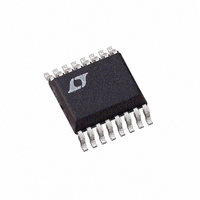
LTC2436-1IGN Linear Technology, LTC2436-1IGN Datasheet - Page 5

LTC2436-1IGN
Manufacturer Part Number
LTC2436-1IGN
Description
IC CONV A/D 16B 2CH DIFF 16SSOP
Manufacturer
Linear Technology
Datasheet
1.LTC2436-1CGN.pdf
(28 pages)
Specifications of LTC2436-1IGN
Number Of Bits
16
Sampling Rate (per Second)
6.8
Data Interface
MICROWIRE™, Serial, SPI™
Number Of Converters
1
Power Dissipation (max)
1mW
Voltage Supply Source
Single Supply
Operating Temperature
-40°C ~ 85°C
Mounting Type
Surface Mount
Package / Case
16-SSOP (0.150", 3.90mm Width)
Lead Free Status / RoHS Status
Contains lead / RoHS non-compliant
Available stocks
Company
Part Number
Manufacturer
Quantity
Price
Company:
Part Number:
LTC2436-1IGN
Manufacturer:
LT
Quantity:
10 000
Part Number:
LTC2436-1IGN#TRPBF
Manufacturer:
LINEAR/凌特
Quantity:
20 000
TI I G CHARACTERISTICS
range, otherwise specifications are at T
SYMBOL
f
t
t
t
f
D
f
t
t
t
t
t
t2
t3
t4
t
t
Note 1: Absolute Maximum Ratings are those values beyond which the
life of the device may be impaired.
Note 2: All voltage values are with respect to GND.
Note 3: V
V
V
(CH0
Note 4: F
with f
Note 5: Guaranteed by design, not subject to test.
Note 6: Integral nonlinearity is defined as the deviation of a code from
a precise analog input voltage. Maximum specifications are limited by
the LSB step size (V
specifications are measured from the center of the quantization band.
Note 7: F
(external oscillator).
EOSC
HEO
LEO
CONV
ISCK
ESCK
LESCK
HESCK
DOUT_ISCK
DOUT_ESCK
1
KQMAX
KQMIN
t
t
5
6
REF
INCM
ISCK
W
+
= REF
EOSC
= (IN
or CH1
O
O
U
CC
= 139,800Hz unless otherwise specified.
+
pin tied to GND or to an external conversion clock source
= GND (internal oscillator) or f
+
= 2.7V to 5.5V unless otherwise specified.
– REF
+ IN
+
) and negative (CH0
PARAMETER
External Oscillator Frequency Range
External Oscillator High Period
External Oscillator Low Period
Conversion Time
Internal SCK Frequency
Internal SCK Duty Cycle
External SCK Frequency Range
External SCK Low Period
External SCK High Period
Internal SCK 19-Bit Data Output Time
External SCK 19-Bit Data Output Time
CS to SDO Low Z
CS to SDO High Z
CS to SCK
CS to SCK
SCK
SDO Hold After SCK
SCK Set-Up Before CS
SCK Hold After CS
–
)/2, IN
–
, V
REF
REFCM
/2
to SDO Valid
+
16
and IN
) and the single shot measurement. Typical
= (REF
–
–
are defined as the selected positive
+
or CH1
+ REF
EOSC
–
A
–
) input respectively.
)/2; V
= 25 C. (Note 3)
= 139,800Hz 2%
IN
= IN
+
The
CONDITIONS
F
External Oscillator (Note 10)
Internal Oscillator (Note 9)
External Oscillator (Notes 9, 10)
(Note 9)
(Note 8)
(Note 8)
(Note 8)
Internal Oscillator (Notes 9, 11)
External Oscillator (Notes 9, 10)
(Note 8)
(Note 9)
(Note 8)
(Note 5)
– IN
O
= 0V
–
,
denotes specifications which apply over the full operating temperature
Note 8: The converter is in external SCK mode of operation such that
the SCK pin is used as digital input. The frequency of the clock signal
driving SCK during the data output is f
Note 9: The converter is in internal SCK mode of operation such that
the SCK pin is used as digital output. In this mode of operation the
SCK pin has a total equivalent load capacitance C
Note 10: The external oscillator is connected to the F
oscillator frequency, f
Note 11: The converter uses the internal oscillator.
F
Note 12: 800nV RMS noise is independent of V
performance is limited by the quantization, lowering V
effective resolution.
Note 13: Guaranteed by design and test correlation.
Note 14: The low sleep mode current is valid only when CS is high.
O
= 0V.
EOSC
, is expressed in kHz.
143.8
2.56
0.25
0.25
1.06
MIN
250
250
45
50
15
50
0
0
0
20510/f
152/f
19/f
ESCK
ESCK
EOSC
f
146.7
EOSC
EOSC
17.5
1.09
TYP
and is expressed in kHz.
LTC2436-1
(in kHz)
(in kHz)
/8
(in kHz)
REF
LOAD
. Since the noise
O
149.6
2000
2000
MAX
1.11
REF
390
390
200
200
200
220
= 20pF.
pin. The external
55
50
improves the
UNITS
24361f
5
kHz
kHz
kHz
kHz
ms
ms
ms
ms
ms
ns
ns
ns
ns
ns
ns
ns
ns
ns
ns
%
s
s


