MCP3008-I/P Microchip Technology, MCP3008-I/P Datasheet - Page 14
MCP3008-I/P
Manufacturer Part Number
MCP3008-I/P
Description
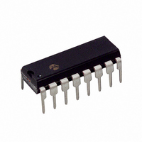
IC ADC 10BIT 2.7V 8CH SPI 16-DIP
Manufacturer
Microchip Technology
Specifications of MCP3008-I/P
Data Interface
Serial, SPI™
Number Of Bits
10
Sampling Rate (per Second)
200k
Number Of Converters
1
Voltage Supply Source
Single Supply
Operating Temperature
-40°C ~ 85°C
Mounting Type
Through Hole
Package / Case
16-DIP (0.300", 7.62mm)
Resolution (bits)
10bit
Sampling Rate
200kSPS
Input Channel Type
Pseudo Differential, Single Ended
Supply Voltage Range - Analog
2.7V To 5.5V
Supply Current
425µA
Lead Free Status / RoHS Status
Lead free / RoHS Compliant
Available stocks
Company
Part Number
Manufacturer
Quantity
Price
Company:

Part Number:
MCP3008-I/P
Manufacturer:
VISHAY
Quantity:
1 001
Part Number:
MCP3008-I/P
Manufacturer:
MICROCHIP/微芯
Quantity:
20 000


MCP3004/3008
4.2
For each device in the family, the reference input
(V
the reference input is reduced, the LSB size is reduced
accordingly.
EQUATION
The theoretical digital output code produced by the A/D
converter is a function of the analog input signal and the
reference input, as shown below.
FIGURE 4-1:
FIGURE 4-2:
Input resistance (R
0.1 LSB deviation in INL from nominal
conditions.
DS21295B-page 14
REF
Legend
VA
4
3
2
1
0
) determines the analog input voltage range. As
100
C
R
CHx
Reference Input
PIN
R
VA
SS
V
T
SS
=
=
=
=
=
CHx
Signal Source
Source Impedance
Input Channel Pad
Input Pin Capacitance
Threshold Voltage
V
f
SAMPLE
DD
Analog Input Model.
Maximum Clock Frequency vs.
Input Resistance (Ohms)
LSB Size
= V
S
REF
= 75 ksps
) to maintain less than a
= 2.7 V
1000
=
7 pF
C
V
------------ -
1024
PIN
REF
V
f
SAMPLE
DD
V
= V
DD
REF
= 200 ksps
I
C
LEAKAGE
SAMPLE
V
V
= 5 V
T
T
= 0.6V
= 0.6V
SS
R
10000
S
=
=
=
=
Leakage Current At The Pin
Due To Various Junctions
sampling switch
sampling switch resistor
sample/hold capacitance
I
±1 nA
LEAKAGE
EQUATION
When using an external voltage reference device, the
system designer should always refer to the manufac-
turer’s recommendations for circuit layout. Any instabil-
ity in the operation of the reference device will have a
direct effect on the operation of the A/D converter.
V
V
IN
REF
= analog input voltage
= reference voltage
Digital Output Code
SS
Sampling
Switch
R
S
= 1 k
2002 Microchip Technology Inc.
V
=
SS
C
= DAC capacitance
= 20 pF
1024
-------------------------- -
SAMPLE
V
REF
V
IN
Related parts for MCP3008-I/P
Image
Part Number
Description
Manufacturer
Datasheet
Request
R

Part Number:
Description:
IC ADC 10BIT 2.7V 8CH SPI 16SOIC
Manufacturer:
Microchip Technology
Datasheet:

Part Number:
Description:
MCP300X 10-Bit Analog-to-Digital Converters
Manufacturer:
Microchip Technology
Datasheet:

Part Number:
Description:
Manufacturer:
Microchip Technology Inc.
Datasheet:
Part Number:
Description:
Manufacturer:
Microchip Technology Inc.
Datasheet:
Part Number:
Description:
Manufacturer:
Microchip Technology Inc.
Datasheet:
Part Number:
Description:
Manufacturer:
Microchip Technology Inc.
Datasheet:
Part Number:
Description:
Manufacturer:
Microchip Technology Inc.
Datasheet:
Part Number:
Description:
Manufacturer:
Microchip Technology Inc.
Datasheet:
Part Number:
Description:
Manufacturer:
Microchip Technology Inc.
Datasheet:
Part Number:
Description:
Manufacturer:
Microchip Technology Inc.
Datasheet: