MCP3008-I/P Microchip Technology, MCP3008-I/P Datasheet - Page 13
MCP3008-I/P
Manufacturer Part Number
MCP3008-I/P
Description
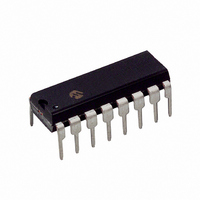
IC ADC 10BIT 2.7V 8CH SPI 16-DIP
Manufacturer
Microchip Technology
Specifications of MCP3008-I/P
Data Interface
Serial, SPI™
Number Of Bits
10
Sampling Rate (per Second)
200k
Number Of Converters
1
Voltage Supply Source
Single Supply
Operating Temperature
-40°C ~ 85°C
Mounting Type
Through Hole
Package / Case
16-DIP (0.300", 7.62mm)
Resolution (bits)
10bit
Sampling Rate
200kSPS
Input Channel Type
Pseudo Differential, Single Ended
Supply Voltage Range - Analog
2.7V To 5.5V
Supply Current
425µA
Lead Free Status / RoHS Status
Lead free / RoHS Compliant
Available stocks
Company
Part Number
Manufacturer
Quantity
Price
Company:

Part Number:
MCP3008-I/P
Manufacturer:
VISHAY
Quantity:
1 001
Part Number:
MCP3008-I/P
Manufacturer:
MICROCHIP/微芯
Quantity:
20 000


3.0
TABLE 3-1:
3.1
Digital ground connection to internal digital circuitry.
3.2
Analog ground connection to internal analog circuitry.
3.3
Analog inputs for channels 0 - 7, respectively, for the
multiplexed inputs. Each pair of channels can be pro-
grammed to be used as two independent channels in
single-ended mode or as a single pseudo-differential
input where one channel is IN+ and one channel is IN.
See Section 4.1, “Analog Inputs”, and Section 5.0,
“Serial
programming the channel configuration.
3.4
The SPI clock pin is used to initiate a conversion and
clock out each bit of the conversion as it takes place.
See Section 6.2, “Maintaining Minimum Clock Speed”,
for constraints on clock speed.
3.5
The SPI port serial data input pin is used to load
channel configuration data into the device.
3.6
The SPI serial data output pin is used to shift out the
results of the A/D conversion. Data will always change
on the falling edge of each clock as the conversion
takes place.
3.7
The CS/SHDN pin is used to initiate communication
with the device when pulled low. When pulled high, it
will end a conversion and put the device in low power
standby. The CS/SHDN pin must be pulled high
between conversions.
V
DGND
AGND
CH0-CH7
CLK
D
D
CS/SHDN
V
2002 Microchip Technology Inc.
DD
REF
IN
OUT
Name
CH0 - CH7
Serial Clock (CLK)
Serial Data Input (D
Serial Data Output (D
Chip Select/Shutdown (CS/SHDN)
PIN DESCRIPTIONS
DGND
AGND
Communication”,
PIN FUNCTION TABLE
+2.7V to 5.5V Power Supply
Digital Ground
Analog Ground
Analog Inputs
Serial Clock
Serial Data In
Serial Data Out
Chip Select/Shutdown Input
Reference Voltage Input
for
Function
IN
)
OUT
information
)
on
4.0
The MCP3004/3008 A/D converters employ a conven-
tional SAR architecture. With this architecture, a sam-
ple is acquired on an internal sample/hold capacitor for
1.5 clock cycles starting on the first rising edge of the
serial clock once CS has been pulled low. Following
this sample time, the device uses the collected charge
on the internal sample and hold capacitor to produce a
serial 10-bit digital output code. Conversion rates of
100 ksps are possible on the MCP3004/3008. See
Section 6.2, “Maintaining Minimum Clock Speed”, for
information on minimum clock rates. Communication
with the device is accomplished using a 4-wire SPI-
compatible interface.
4.1
The MCP3004/3008 devices offer the choice of using
the analog input channels configured as single-ended
inputs or pseudo-differential pairs. The MCP3004 can
be configured to provide two pseudo-differential input
pairs or four single-ended inputs. The MCP3008 can be
configured to provide four pseudo-differential input
pairs or eight single-ended inputs. Configuration is
done as part of the serial command before each con-
version begins. When used in the pseudo-differential
mode, each channel pair (i.e., CH0 and CH1, CH2 and
CH3 etc.) are programmed as the IN+ and IN- inputs as
part of the command string transmitted to the device.
The IN+ input can range from IN- to (V
IN- input is limited to ±100 mV from the V
input can be used to cancel small signal common-
mode noise, which is present on both the IN+ and IN-
inputs.
When operating in the pseudo-differential mode, if the
voltage level of IN+ is equal to or less than IN-, the
resultant code will be 000h. If the voltage at IN+ is
equal to or greater than {[V
the output code will be 3FFh. If the voltage level at IN-
is more than 1 LSB below V
IN+ input will have to go below V
output code. Conversely, if IN- is more than 1 LSB
above V
IN+ input level goes above V
For the A/D converter to meet specification, the charge
holding capacitor (C
time to acquire a 10-bit accurate voltage level during
the 1.5 clock cycle sampling period. The analog input
model is shown in Figure 4-1.
This diagram illustrates that the source impedance (R
adds to the internal sampling switch (R
directly affecting the time that is required to charge the
capacitor (C
impedances increase the offset, gain and integral lin-
earity errors of the conversion (see Figure 4-2).
SS
DEVICE OPERATION
Analog Inputs
, the 3FFh code will not be seen unless the
SAMPLE
MCP3004/3008
). Consequently, larger source
SAMPLE
REF
SS
) must be given enough
REF
, the voltage level at the
+ (IN-)] - 1 LSB}, then
level.
SS
DS21295B-page 13
to see the 000h
SS
REF
SS
) impedance,
rail. The IN-
+ IN-). The
S
)
Related parts for MCP3008-I/P
Image
Part Number
Description
Manufacturer
Datasheet
Request
R

Part Number:
Description:
IC ADC 10BIT 2.7V 8CH SPI 16SOIC
Manufacturer:
Microchip Technology
Datasheet:

Part Number:
Description:
MCP300X 10-Bit Analog-to-Digital Converters
Manufacturer:
Microchip Technology
Datasheet:

Part Number:
Description:
Manufacturer:
Microchip Technology Inc.
Datasheet:
Part Number:
Description:
Manufacturer:
Microchip Technology Inc.
Datasheet:
Part Number:
Description:
Manufacturer:
Microchip Technology Inc.
Datasheet:
Part Number:
Description:
Manufacturer:
Microchip Technology Inc.
Datasheet:
Part Number:
Description:
Manufacturer:
Microchip Technology Inc.
Datasheet:
Part Number:
Description:
Manufacturer:
Microchip Technology Inc.
Datasheet:
Part Number:
Description:
Manufacturer:
Microchip Technology Inc.
Datasheet:
Part Number:
Description:
Manufacturer:
Microchip Technology Inc.
Datasheet: