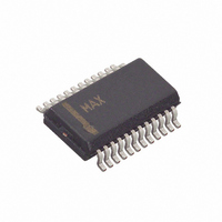
MAX1168BCEG+ Maxim Integrated Products, MAX1168BCEG+ Datasheet - Page 22

MAX1168BCEG+
Manufacturer Part Number
MAX1168BCEG+
Description
IC ADC 16BIT 200KSPS 24-QSOP
Manufacturer
Maxim Integrated Products
Datasheet
1.MAX1167BEEE.pdf
(30 pages)
Specifications of MAX1168BCEG+
Number Of Bits
16
Sampling Rate (per Second)
200k
Data Interface
MICROWIRE™, QSPI™, Serial, SPI™
Number Of Converters
1
Power Dissipation (max)
762mW
Voltage Supply Source
Analog and Digital
Operating Temperature
0°C ~ 70°C
Mounting Type
Surface Mount
Package / Case
24-QSOP
Lead Free Status / RoHS Status
Lead free / RoHS Compliant
setting bits 4 and 3 in the command/configuration/con-
trol register (see Tables 3 and 4). In scan mode, conver-
sion results are stored in memory until the completion of
the last conversion in the sequence. Upon completion of
the last conversion in the sequence, EOC transitions
from high to low to indicate the end of the conversion
and shuts down the internal oscillator. Use the EOC
high-to-low transition as the signal to restart the external
clock (SCLK). DOUT provides the conversion results in
the same order as the channel conversion process. The
MSB of the first conversion is available at DOUT on the
falling edge of EOC. Figure 15 shows the timing
diagram for 16-bit-wide data transfer in scan mode.
Figure 16 shows the DSP-interface timing diagram.
Logic low at DSPR on the falling edge of CS enables
DSP interface mode. After the MAX1168 enters DSP
mode, CS can remain low for the duration of the conver-
sion process and each subsequent conversion. Drive
DSEL low to select the 8-bit data-transfer mode. A sync
pulse from the DSP at DSPR wakes the analog circuitry
and allows SCLK to clock in data (Figure 17). The frame
sync pulse alerts the MAX1168 that incoming data is
about to be sent to DIN. Ensure the duty cycle on SCLK
is between 45% and 55% when operating at 4.8MHz
(the maximum clock frequency). For lower clock fre-
quencies, ensure the minimum high and low times are at
least 93ns. External clock mode conversions with SCLK
Multichannel, 16-Bit, 200ksps Analog-to-Digital
Converters
Figure 19. Unipolar Transfer Function, Full Scale (FS) = V
Zero Scale (ZS) = GND
22
DSP 8-Bit-Wide Data-Transfer Mode (External Clock
______________________________________________________________________________________
1111...111
1111...110
1111...101
0000...011
0000...010
0000...001
0000...000
OUTPUT CODE
0
1
2
INPUT VOLTAGE (LSB)
3
TRANSITION
FULL-SCALE
Mode, MAX1168 Only)
FS - 3/2 LSB
1 LSB =
FS = V
FS
65,536
V
REF
REF
REF
,
rates less than 125kHz can reduce accuracy due to
leakage of the sampling capacitor. The input data
latches on the falling edge of SCLK. The command/
configuration/control register starts reading data in on
the falling edge of the first SCLK cycle immediately fol-
lowing the falling edge of the frame sync pulse and
ends on the falling edge of the 8th SCLK cycle. The
MAX1168 selects the proper channel for conversion on
the falling edge of the 3rd clock cycle and begins
acquisition. Acquisition continues until the rising edge
of the 7th clock cycle. The MAX1168 samples the input
on the rising edge of the 7th clock cycle. On the rising
edge of the 8th clock cycle, the MAX1168 outputs a
frame sync pulse at DSPX. The frame sync pulse alerts
the DSP that the conversion results are about to be out-
put at DOUT (MSB first) starting on the rising edge of
the 9th clock pulse. To read the entire conversion
result, 16 SCLK cycles are needed. Extra clock pulses,
occurring after the conversion result has been clocked
out and prior to the next rising edge of DSPR, cause
zeros to be clocked out of DOUT. The MAX1168 exter-
nal clock, DSP 8-bit-wide data-transfer mode requires
24 clock cycles to complete.
Begin a new conversion by sending a new frame sync
pulse to DSPR followed by new configuration data.
Send the new DSPR pulse immediately after reading
the conversion result to realize maximum throughput.
Sending a new frame sync pulse in the middle of a con-
version immediately aborts the current conversion and
begins a new one. A rising edge on CS in the middle of
a conversion aborts the current conversion and places
the MAX1168 in shutdown.
Figure 16 shows the DSP-interface timing diagram.
Logic low at DSPR on the falling edge of CS enables
DSP interface mode. After the MAX1168 enters DSP
mode, CS can remain low for the duration of the con-
version process and each subsequent conversion. The
acquisition time is extended an extra eight SCLK cycles
in the 16-bit-wide data-transfer mode. Drive DSEL high
to select the 16-bit-wide data-transfer mode. A sync
pulse from the DSP at DSPR wakes the analog circuitry
and allows SCLK to clock in data (Figure 18). The
frame sync pulse also alerts the MAX1168 that incom-
ing data is about to be sent to DIN. Ensure the duty
cycle on SCLK is between 45% and 55% when operat-
ing at 4.8MHz (the maximum clock frequency). For
lower clock frequencies, ensure the minimum high and
low times are at least 93ns. External-clock-mode con-
versions with SCLK rates less than 125kHz can reduce
accuracy due to leakage of the sampling capacitor.
DSP 16-Bit-Wide Data-Transfer Mode (External
Clock Mode, MAX1168 Only)


