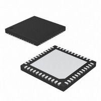
MAX19516ETM+ Maxim Integrated Products, MAX19516ETM+ Datasheet - Page 18

MAX19516ETM+
Manufacturer Part Number
MAX19516ETM+
Description
IC ADC 10BIT 100MSPS DUAL 48TQFN
Manufacturer
Maxim Integrated Products
Datasheet
1.MAX19516ETM.pdf
(35 pages)
Specifications of MAX19516ETM+
Number Of Bits
10
Sampling Rate (per Second)
100M
Data Interface
Serial, Parallel
Number Of Converters
2
Voltage Supply Source
Analog and Digital
Operating Temperature
-40°C ~ 85°C
Mounting Type
Surface Mount
Package / Case
48-TQFN Exposed Pad
Conversion Rate
100 MSPs
Resolution
10 bit
Interface Type
SPI
Snr
60.1 dB
Voltage Reference
1.25 V
Supply Voltage (max)
3.5 V
Supply Voltage (min)
1.7 V
Maximum Power Dissipation
3200 mW
Maximum Operating Temperature
+ 85 C
Mounting Style
SMD/SMT
Input Voltage
1.8 V
Minimum Operating Temperature
- 40 C
Lead Free Status / RoHS Status
Lead free / RoHS Compliant
Dual-Channel, 10-Bit, 100Msps ADC
In addition to power management, the HPS_SHDN1
and HPS_SHDN0 activate an A+B adder mode. In this
mode, the results from both channels are averaged.
Control Bits:
Output Format (01h)
* HPS_SHDN0, STBY_SHDN0, CHA_ON_SHDN0, and CHB_ON_SHDN0 are active when SHDN = 0.
** HPS_SHDN1, STBY_SHDN1, CHA_ON_SHDN1, and CHB_ON_SHDN1 are active when SHDN = 1.
X = Don’t care.
Note: When HPS_SHDN_ = 1 (A+B adder mode), CHA_ON_SHDN_ and CHB_ON_SHDN_ must BOTH equal 0 for power-down or
standby.
Bit 7, 6, 5
Bit 4
Bit 3
Bit 2
Bit 1
Bit 0
18
HPS_SHDN0
HPS_SHDN1
BIT 7
______________________________________________________________________________________
0
X
0
0
0
0
0
0
1
1
1
Set to 0 for proper operation
BIT_ORDER_B: Reverse CHB output bit order
0 = Defined data bus pin order (default)
1 = Reverse data bus pin order
BIT_ORDER_A: Reverse CHA output bit order
0 = Defined data bus pin order (default)
1 = Reverse data bus pin order
MUX_CH: Multiplexed data bus selection
0 = Multiplexed data output on CHA (CHA data presented first, followed by CHB data) (default)
1 = Multiplexed data output on CHB (CHB data presented first, followed by CHA data)
MUX: Digital output mode
0 = Dual data bus output mode (default)
1 = Single multiplexed data bus output mode
Set to 0 for proper operation
BIT 6
MUX_CH selects the output bus
0
STBY_SHDN0
STBY_SHDN1
X
X
X
0
0
0
1
1
1
1
BIT 5
0
CHA_ON_SHDN0
CHA_ON_SHDN1
BIT_ORDER_B
X
0
0
1
1
0
0
1
0
1
BIT 4
CHB_ON_SHDN0
CHB_ON_SHDN1
The MUX_CH bit selects which bus the (A+B)/2 data is
presented.
X
BIT_ORDER_A
0
1
0
1
0
1
0
0
1
BIT 3
Complete power-down
Channel B active, channel A full power-down
Channel A active, channel B full power-down
Channels A and B active
Channels A and B in standby mode
Channel B active, channel A standby
Channel A active, channel B standby
Channels A and B in standby mode
Channels A and B active, output is averaged
Channels A and B active, output is averaged
MUX_CH
BIT 2
SHDN INPUT = 1**
SHDN INPUT = 0*
BIT 1
MUX
BIT 0
0


