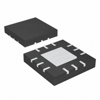
MAX1277AETC+ Maxim Integrated Products, MAX1277AETC+ Datasheet - Page 2

MAX1277AETC+
Manufacturer Part Number
MAX1277AETC+
Description
IC ADC 12BIT 1.5MSPS 12-TQFN
Manufacturer
Maxim Integrated Products
Datasheet
1.MAX1277AETC.pdf
(18 pages)
Specifications of MAX1277AETC+
Number Of Bits
12
Sampling Rate (per Second)
1.5M
Data Interface
MICROWIRE™, QSPI™, Serial, SPI™
Number Of Converters
1
Power Dissipation (max)
1.35W
Voltage Supply Source
Analog and Digital
Operating Temperature
-40°C ~ 85°C
Mounting Type
Surface Mount
Package / Case
12-WQFN Exposed Pad
Lead Free Status / RoHS Status
Lead free / RoHS Compliant
ABSOLUTE MAXIMUM RATINGS
V
V
Digital Inputs
Digital Output
Analog Inputs and
RGND to GND .......................................................-0.3V to +0.3V
ELECTRICAL CHARACTERISTICS
(V
at T
1.5Msps, Single-Supply, Low-Power, True-
Differential, 12-Bit ADCs with Internal Reference
Stresses beyond those listed under “Absolute Maximum Ratings” may cause permanent damage to the device. These are stress ratings only, and functional
operation of the device at these or any other conditions beyond those indicated in the operational sections of the specifications is not implied. Exposure to
absolute maximum rating conditions for extended periods may affect device reliability.
2
DD
L
DC ACCURACY
Resolution
Relative Accuracy (Note 1)
Differential Nonlinearity (Note 2)
Offset Error
Offset-Error Temperature
Coefficient
Gain Error
Gain Temperature Coefficient
DYNAMIC SPECIFICATIONS (f
Signal-to-Noise Plus Distortion
Total Harmonic Distortion
Spurious-Free Dynamic Range
Intermodulation Distortion
Full-Power Bandwidth
Full-Linear Bandwidth
CONVERSION RATE
Minimum Conversion Time
Maximum Throughput Rate
M i ni m um Thr oug hp ut Rate
Track-and-Hold Acquisition Time
Aperture Delay
Aperture Jitter
External Clock Frequency
DD
to GND .................-0.3V to the lower of (V
to GND ....................-0.3V to the lower of (V
REF to GND..........-0.3V to the lower of (V
to GND ................-0.3V to the lower of (V
A
_______________________________________________________________________________________
to GND ..............................................................-0.3V to +6V
= +2.7V to +3.6V, V
= +25°C.)
PARAMETER
L
= V
DD
IN
, f
SCLK
= 525kHz sine wave, V
SYMBOL
SINAD
t
SFDR
f
CONV
t
DNL
THD
SCLK
IMD
= 24MHz, 50% duty cycle, T
INL
ACQ
DD
DD
DD
L
+ 0.3V) and +6V
+ 0.3V) and +6V
+ 0.3V) and +6V
+ 0.3V) and +6V
MAX127_A
MAX127_B
MAX127_A
MAX127_B
Offset nulled
Up to the 5th harmonic
f
-3dB point, small-signal method
S/(N + D) > 68dB, single ended
(Note 3)
( N ote 4)
(Note 5)
(Note 6)
(Note 7)
IN1
= 250kHz, f
IN
= V
REF
CONDITIONS
IN2
, unless otherwise noted.)
Maximum Current into Any Pin............................................50mA
Continuous Power Dissipation (T
Operating Temperature Range
Junction Temperature ......................................................+150°C
Storage Temperature Range .............................-60°C to +150°C
Lead Temperature (soldering, 10s) .................................+300°C
= 300kHz
A
= -40°C to +85°C, unless otherwise noted. Typical values are
12-Pin TQFN (derate 16.9mW/°C above +70°C) ......1349mW
MAX127_ _ ETC ..............................................-40°C to +85°C
MIN
-1.0
-1.5
-1.0
-1.0
1.5
12
66
10
A
= +70°C)
TYP
68.5
125
-80
-83
-78
1.2
±1
±2
15
30
5
0.667
MAX
+1.0
+1.5
+1.0
+1.5
±8.0
±6.0
-76
-76
24
ppm/°C
ppm/°C
UNITS
Msps
MHz
MHz
ksps
MHz
LSB
LSB
LSB
LSB
Bits
dB
dB
dB
dB
µs
ns
ns
ps


