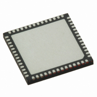
MAX11045ETN+ Maxim Integrated Products, MAX11045ETN+ Datasheet - Page 18

MAX11045ETN+
Manufacturer Part Number
MAX11045ETN+
Description
ADC 16BIT SAMPLING 6CH 56-TQFN
Manufacturer
Maxim Integrated Products
Datasheet
1.MAX11044ETN.pdf
(27 pages)
Specifications of MAX11045ETN+
Number Of Bits
16
Sampling Rate (per Second)
250k
Data Interface
Parallel
Number Of Converters
6
Power Dissipation (max)
2.22W
Voltage Supply Source
Analog and Digital
Operating Temperature
-40°C ~ 85°C
Mounting Type
Surface Mount
Package / Case
56-WQFN Exposed Pad, 56-HWQFN
Number Of Adc Inputs
6
Architecture
SAR
Conversion Rate
250 KSPs
Resolution
16 bit
Input Type
Voltage
Interface Type
Parallel
Snr
92.3 dB
Voltage Reference
Internal 4.096 V
Supply Voltage (max)
5.25 V
Supply Voltage (min)
2.7 V, 4.75 V
Maximum Power Dissipation
2222 mW
Maximum Operating Temperature
+ 85 C
Mounting Style
SMD/SMT
Input Voltage
5 V
Minimum Operating Temperature
- 40 C
Lead Free Status / RoHS Status
Lead free / RoHS Compliant
4-/6-/8-Channel, 16-/14-Bit,
Simultaneous-Sampling ADCs
CONVST initiates conversions. The MAX11044/
MAX11045/MAX11046 and MAX11054/MAX11055/
MAX11056 provide two acquisition modes set through
the configuration register. Allow a quiet time (t
500ns prior to the start of conversion to avoid any noise
interference during readout or write operations from
corrupting a sample.
In default mode (CR0 = 0), drive CONVST low to place
the MAX11044/MAX11045/MAX11046 and MAX11054/
MAX11055/MAX11056 into acquisition mode. All the
input switches are closed and the internal T/H circuits
track the respective input voltage. Keep the CONVST
signal low for at least 1µs (t
tling of the sampled voltages. On the rising edge of
CONVST, the switches are opened and the
MAX11044/MAX11045/MAX11046 and MAX11054/
MAX11055/MAX11056 begin the conversion on all the
samples in parallel. EOC remains high until the conver-
sion is completed.
In the second mode (CR0 = 1), the MAX11044/
MAX11045/MAX11046 and MAX11054/MAX11055/
MAX11056 enter acquisition mode as soon as the previ-
ous conversion is completed. CONVST rising edge initi-
ates the next sample and conversion sequence.
CONVST needs to be low for at least 20ns to be valid.
Provide adequate time for acquisition and the requisite
quiet time in both modes to achieve accurate sampling
and maximum performance of the MAX11044/
MAX11045/MAX11046 and MAX11054/MAX11055/
MAX11056.
Figure 4. Programming Configuration-Register Timing
Requirements
18
______________________________________________________________________________________
(USER SUPPLIED)
(USER SUPPLIED)
(USER SUPPLIED)
CR0–CR3
WR
CS
t
3
Starting a Conversion
ACQ
CONFIGURATION
t
4
REGISTER
) to enable proper set-
t
6
t
7
t
5
Q
) of
The CS and RD are active-low, digital inputs that con-
trol the readout through the 16-/14-bit, parallel, 20MHz
data bus (D0–D15/D13). After EOC transitions low, read
the conversion data by driving CS and RD low. Each
low period of RD presents the next channel’s result.
When CS or RD are high, the data bus is high imped-
ance. CS may be driven high between individual chan-
nel readouts or left low during the entire 8-channel
readout.
The MAX11044/MAX11045/MAX11046 and MAX11054/
MAX11055/MAX11056 feature a precision, low-drift,
internal bandgap reference. Bypass REFIO with a 0.1µF
capacitor to AGND to reduce noise. The REFIO output
voltage may be used as a reference for other circuits. The
output impedance of REFIO is 10kΩ. Drive only high
impedance circuits or buffer externally when using REFIO
to drive external circuitry.
Set the configuration register to disable the internal ref-
erence and drive REFIO with a high-quality external ref-
erence. To avoid signal degradation, ensure that the
integrated reference noise applied to REFIO is less
than 10µV in the bandwidth of up to 50kHz.
Figure 5. Readout Timing Requirements
(USER SUPPLIED)
(USER SUPPLIED)
DB0–DB15/DB13
CS
RD
t
8
Reading Conversion Results
t
12
t
9
S
n
t
10
t
13
t
11
External Reference
Internal Reference
Reference
S
n + 1


