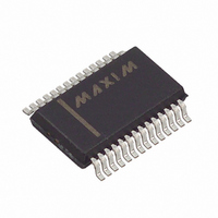
MAX1496EAI+ Maxim Integrated Products, MAX1496EAI+ Datasheet - Page 17

MAX1496EAI+
Manufacturer Part Number
MAX1496EAI+
Description
IC ADC 3.5DIGIT LED DRVR 28-SSOP
Manufacturer
Maxim Integrated Products
Datasheet
1.MAX1496EAI.pdf
(24 pages)
Specifications of MAX1496EAI+
Number Of Bits
3.5 Digit
Sampling Rate (per Second)
5
Number Of Converters
1
Voltage Supply Source
Analog and Digital
Operating Temperature
-40°C ~ 85°C
Mounting Type
Surface Mount
Package / Case
28-SSOP
Lead Free Status / RoHS Status
Lead free / RoHS Compliant
The transfer function for the MAX1496 with AIN+ - AIN-
≥ 0, RANGE = GND is:
The transfer function for the MAX1496 with AIN+ - AIN-
< 0, RANGE = GND is:
The transfer function for the MAX1496 with AIN+ - AIN-
≥ 0, RANGE = V
The transfer function for the MAX1496 with AIN+ - AIN-
< 0, RANGE = V
Figure 12. MAX1496 Transfer Function, ±200mV Range
COUNT
COUNT
COUNT
- 1 - - -
COUNT
1 - - -
-1999
LED
- 0
- 1
- 2
1999
2
1
0
=
=
=
1 024
-200mV
1 024
.
1 024
=
.
DD
DD
.
1 024
______________________________________________________________________________________
.
is:
is:
V
V
REF
V
AIN
V
V
V
REF
AIN
REF
ANALOG INPUT VOLTAGE
AIN
+
+
V
V
-100µV 100µV
REF
+
+
AIN
−
−
+
+
V
V
−
−
−
−
REF
AIN
V
V
3.5- and 4.5-Digit, Single-Chip ADCs
+
+
V
V
0
REF
AIN
REF
AIN
−
−
−
−
V
V
REF
−
AIN
−
−
−
×
×
−
−
×
2000
×
2000
2000
2000
+200mV
×
×
+
10
1
10
+
1
Power up AV
V
external-reference voltage to the device. If this is not
possible, limit the current into these inputs to 50mA.
When the analog and digital supplies come from the
same source, isolate the digital supply from the analog
supply with a low-value resistor (10Ω) or ferrite bead.
For best performance, ground the MAX1447/
MAX1496/MAX1498 to the analog ground plane of the
circuit board.
Avoid running digital lines under the device as this can
couple noise onto the IC. Run the analog ground plane
under the MAX1447/MAX1496/MAX1498 to minimize
coupling of digital noise. Make the power-supply lines
to the MAX1447/MAX1496/MAX1498 as wide as possi-
ble to provide low-impedance paths and reduce the
effects of glitches on the power-supply line.
Shield fast-switching signals, such as clocks, with digital
ground to avoid radiating noise to other sections of the
board. Avoid running clock signals near the analog
inputs. Avoid crossover of digital and analog signals.
Running traces that are on opposite sides of the board at
right angles to each other reduces feedthrough effects.
Good decoupling is important when using high-resolution
ADCs. Decouple the supplies with 0.1µF ceramic capaci-
tors to GND. Place these components as close to the
device as possible to achieve the best decoupling.
Figure 13. MAX1496 Transfer Function, ±2V Range
DD
(MAX1496) before applying an analog input and
- 1 - - -
1 - - -
-1999
LED
- 0
- 1
- 2
1999
2
1
0
DD
Supplies, Layout, and Bypassing
with LED Drivers
-2V
and DV
ANALOG INPUT VOLTAGE
DD
-1mV
(MAX1447/MAX1498) and
0
1mV
+2V
17


