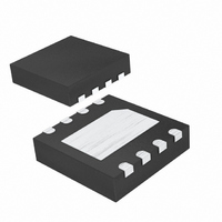
MAX1086ETA+T Maxim Integrated Products, MAX1086ETA+T Datasheet - Page 8

MAX1086ETA+T
Manufacturer Part Number
MAX1086ETA+T
Description
IC ADC 10BIT 150KSPS 8-TDFN
Manufacturer
Maxim Integrated Products
Datasheet
1.MAX1086ETAT.pdf
(15 pages)
Specifications of MAX1086ETA+T
Number Of Bits
10
Sampling Rate (per Second)
150k
Data Interface
MICROWIRE™, QSPI™, Serial, SPI™
Number Of Converters
1
Power Dissipation (max)
1.6mW
Voltage Supply Source
Single Supply
Operating Temperature
-40°C ~ 85°C
Mounting Type
Surface Mount
Package / Case
8-WDFN Exposed Pad
Number Of Adc Inputs
2
Architecture
SAR
Conversion Rate
150 KSPs
Resolution
10 bit
Input Type
Differential
Interface Type
3-Wire (SPI, QSPI, MICROWIRE)
Voltage Reference
External
Supply Voltage (max)
5 V
Maximum Power Dissipation
1454.5 mW
Maximum Operating Temperature
+ 85 C
Mounting Style
SMD/SMT
Minimum Operating Temperature
- 40 C
Lead Free Status / RoHS Status
Lead free / RoHS Compliant
Other names
MAX1086ETA+T
150ksps, 10-Bit, 2-Channel Single-Ended, and
1-Channel True-Differential ADCs in SOT23 and TDFN
Figure 4. Equivalent Input Circuit
where R
input signal, and t
device.
Note: t
impedance below 300Ω does not significantly affect the
ADC‘s AC performance. A high impedance source can
be accommodated either by lengthening t
placing a 1µF capacitor between the positive and neg-
ative analog inputs.
Select between the MAX1086/MAX1087’s two positive
input channels using the CNVST pin. If AIN1 is desired
(Figure 5a), drive CNVST high to power-up the ADC
and place the T/H in track mode with AIN1 connected
to the positive input capacitor. Hold CNVST high for
t
place the T/H in hold mode. The ADC will then perform
a conversion and shutdown automatically. The MSB is
available at DOUT after 3.7µs. Data can then be
clocked out using SCLK. Be sure to clock out all 12 bits
of data (the 10-bit result plus two sub-bits) before dri-
ving CNVST high for the next conversion. If all 12 bits of
data are not clocked out before CNVST is driven high,
AIN2 will be selected for the next conversion.
If AIN2 is desired (Figure 5b), drive CNVST high for at
least 30ns. Next, drive it low for at least 30ns, and then
high again. This will power-up the ADC and place the
T/H in track mode with AIN2 connected to the positive
input capacitor. Now hold CNVST high for t
acquire the signal. Drive CNVST low to place the T/H in
hold mode. The ADC will then perform a conversion
and shutdown automatically. The MSB is available at
8
ACQ
*( ) APPLIES TO MAX1088/1089
_______________________________________________________________________________________
AIN1(AIN+)
to fully acquire the signal. Drive CNVST low to
GND(AIN-)
ACQ
IN
AIN2
= 1.5kΩ, R
HOLD
is never less than 1.4µs and any source
PWR
GND
REF
S
= 1µs is the power-up time of the
V
is the source impedance of the
HOLD
CIN+
CIN-
DD
Selecting AIN1 or AIN2
/2
RIN-
(MAX1086/MAX1087)
DAC
TRACK
RIN+
COMPARATOR
HOLD
ACQ
+
-
ACQ
to fully
or by
DOUT after 3.7µs. Data can then be clocked out using
SCLK. If all 12 bits of data are not clocked out before
CNVST is driven high, AIN2 will be selected for the next
conversion.
Initiate true-differential conversions with the
MAX1088/MAX1089’s unipolar and bipolar modes,
using the CNVST pin. AIN+ and AIN- are sampled at
the falling edge of CNVST. In unipolar mode, AIN+ can
exceed AIN- by up to V
straight binary. In bipolar mode, either input can
exceed the other by up to V
two’s complement.
Note: In both modes, AIN+ and AIN- must not exceed
V
than 50mV.
If unipolar mode is desired (Figure 5a), drive CNVST
high to power-up the ADC and place the T/H in track
mode with AIN+ and AIN- connected to the input
capacitors. Hold CNVST high for t
the signal. Drive CNVST low to place the T/H in hold
mode. The ADC will then perform a conversion and
shutdown automatically. The MSB is available at DOUT
after 3.7µs. Data can then be clocked out using SCLK.
Be sure to clock out all 12 bits (the 10-bit result plus
two sub-bits) of data before driving CNVST high for the
next conversion. If all 12 bits of data are not clocked
out before CNVST is driven high, bipolar mode will be
selected for the next conversion.
If bipolar mode is desired (Figure 5b), drive CNVST
high for at least 30ns. Next, drive it low for at least 30ns
and then high again. This will place the T/H in track
mode with AIN+ and AIN- connected to the input
capacitors. Now hold CNVST high for t
acquire the signal. Drive CNVST low to place the T/H in
hold mode. The ADC will then perform a conversion
and shutdown automatically. The MSB is available at
DOUT after 3.7µs. Data can then be clocked out using
SCLK. If all 12 bits of data are not clocked out before
CNVST is driven high, bipolar mode will be selected for
the next conversion.
The ADCs input tracking circuitry has a 1MHz small-
signal bandwidth, so it is possible to digitize high-
speed transient events and measure periodic signals
with bandwidths exceeding the ADC’s sampling rate by
using undersampling techniques. To avoid high fre-
quency signals being aliased into the frequency band
of interest, anti-alias filtering is recommended.
DD
Selecting Unipolar or Bipolar Conversions
by more than 50mV or be lower than GND by more
REF
REF
(MAX1088/MAX1089)
. The output format is
/2. The output format is
Input Bandwidth
ACQ
to fully acquire
ACQ
to fully


