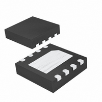
MAX1086ETA+T Maxim Integrated Products, MAX1086ETA+T Datasheet - Page 12

MAX1086ETA+T
Manufacturer Part Number
MAX1086ETA+T
Description
IC ADC 10BIT 150KSPS 8-TDFN
Manufacturer
Maxim Integrated Products
Datasheet
1.MAX1086ETAT.pdf
(15 pages)
Specifications of MAX1086ETA+T
Number Of Bits
10
Sampling Rate (per Second)
150k
Data Interface
MICROWIRE™, QSPI™, Serial, SPI™
Number Of Converters
1
Power Dissipation (max)
1.6mW
Voltage Supply Source
Single Supply
Operating Temperature
-40°C ~ 85°C
Mounting Type
Surface Mount
Package / Case
8-WDFN Exposed Pad
Number Of Adc Inputs
2
Architecture
SAR
Conversion Rate
150 KSPs
Resolution
10 bit
Input Type
Differential
Interface Type
3-Wire (SPI, QSPI, MICROWIRE)
Voltage Reference
External
Supply Voltage (max)
5 V
Maximum Power Dissipation
1454.5 mW
Maximum Operating Temperature
+ 85 C
Mounting Style
SMD/SMT
Minimum Operating Temperature
- 40 C
Lead Free Status / RoHS Status
Lead free / RoHS Compliant
Other names
MAX1086ETA+T
the first eight data bits starting with the MSB. The sec-
ond 8-bit data stream contains the remaining bits, D1
through D0, and the two sub-bits S1 and S0.
For best performance, use printed circuit (PC) boards.
Wire-wrap configurations are not recommended since
the layout should ensure proper separation of analog
150ksps, 10-Bit, 2-Channel Single-Ended, and
1-Channel True-Differential ADCs in SOT23 and TDFN
Figure 8c. SPI/MICROWIRE Interface Timing Sequence (CPOL = CPHA = 0)
Figure 9a. QSPI Connections
12
Table 2. Detailed SSPSTAT Register Content
X = Don’t care
CNVST
SCLK
DOUT
SMP
CKE
CONTROL BIT
R/W
D/A
UA
BF
______________________________________________________________________________________
P
S
Layout, Grounding, and Bypassing
QSPI
Bit 7
Bit 6
Bit 5
Bit 4
Bit 3
Bit 2
Bit 1
Bit 0
MSB
B9
MISO
SAMPLING INSTANT
1
SCK
CS
SS
MAX1086–MAX1089
B8
SETTINGS
V
DD
B7
1ST BYTE READ
0
1
X
X
X
X
X
X
B6
4
CNVST
SCLK
DOUT
B5
MAX1086–
MAX1089
SPI Data Input Sample Phase. Input data is sampled at the middle of the data output
time.
SPI Clock Edge Select Bit. Data will be transmitted on the rising edge of the serial clock.
Data Address Bit
Stop Bit
Start Bit
Read/Write Bit Information
Update Address
Buffer Full Status Bit
B4
SYNCHRONOUS SERIAL STATUS REGISTER (SSPSTAT)
B3
B2
8
and digital traces. Do not run analog and digital lines
parallel to each other, and do not lay out digital signal
paths underneath the ADC package. Use separate
analog and digital PC board ground sections with only
one starpoint (Figure 11), connecting the two ground
systems (analog and digital). For lowest-noise opera-
tion, ensure the ground return to the star ground’s
power supply is low impedance and as short as possi-
ble. Route digital signals far away from sensitive analog
and reference inputs.
High-frequency noise in the power supply (V
degrade the performance of the ADC’s fast comparator.
Bypass V
located as close as possible to the MAX1086–MAX1089s
power supply pin. Minimize capacitor lead length for best
supply-noise rejection. Add an attenuation resistor (5Ω) if
the power supply is extremely noisy.
B1
DD
LSB
B0
to the star ground with a 0.1µF capacitor,
S1
S0
12
2ND BYTE READ
HIGH-Z
DD
16
) may


