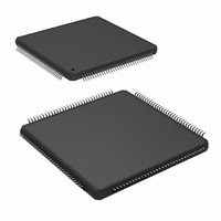
ADC083000CIYB/NOPB National Semiconductor, ADC083000CIYB/NOPB Datasheet - Page 7

ADC083000CIYB/NOPB
Manufacturer Part Number
ADC083000CIYB/NOPB
Description
IC ADC 8BIT 3GSPS LP 128-LQFP
Manufacturer
National Semiconductor
Series
PowerWise®r
Datasheet
1.ADC083000CIYBNOPB.pdf
(40 pages)
Specifications of ADC083000CIYB/NOPB
Number Of Bits
8
Sampling Rate (per Second)
3G
Data Interface
Serial
Number Of Converters
2
Power Dissipation (max)
2.3W
Voltage Supply Source
Single Supply
Operating Temperature
-40°C ~ 85°C
Mounting Type
Surface Mount
Package / Case
128-LQFP Exposed Pad
Lead Free Status / RoHS Status
Lead free / RoHS Compliant
Other names
*ADC083000CIYB
*ADC083000CIYB/NOPB
ADC083000CIYB
*ADC083000CIYB/NOPB
ADC083000CIYB
Available stocks
Company
Part Number
Manufacturer
Quantity
Price
Company:
Part Number:
ADC083000CIYB/NOPB
Manufacturer:
IPS
Quantity:
2 300
Part Number:
ADC083000CIYB/NOPB
Manufacturer:
TI/德州仪器
Quantity:
20 000
Pin Functions
100 / 101
102 / 103
104 / 105
106 / 107
111 / 112
113 / 114
115 / 116
117 / 118
122 / 123
124 / 125
Pin No.
36 / 37
38 / 39
43 / 44
45 / 46
47 / 48
49 / 50
54 / 55
56 / 57
58 / 59
60 / 61
65 / 66
67 / 68
69 / 70
71 / 72
75 / 76
77 / 78
83 / 84
85 / 86
89 / 90
91 / 92
93 / 94
95 / 96
79
80
82
81
Da2+ / Da2−
Da4+ / Da4−
Da6+ / Da6−
Dd7− / Dd7+
Dd5− / Dd5+
Dd1− / Dd1+
Db5− / Db5+
Db3− / Db3+
Db1− / Db1+
Dc2+ / Dc2−
Dc4+ / Dc4−
Dc6+ / Dc6−
Da0+ / Da0-
Da1+ / Da1-
Da3+ / Da3-
Da5+ / Da5-
Da7+ / Da7-
Dd6- / Dd6+
Dd4- / Dd4+
Dd3- / Dd3+
Dd2- / Dd2+
Dd0- / Dd0+
Db7- / Db7+
Db6- / Db6+
Db4- / Db4+
Db2- / Db2+
Db0- / Db0+
Dc0+ / Dc0-
Dc1+ / Dc1-
Dc3+ / Dc3-
Dc5+ / Dc5-
Dc7+ / Dc7-
Symbol
DCLK+
DCLK-
OR+
OR-
Equivalent Circuit
7
A and C Data
(Output):LVDS Data Outputs from the first internal converter.
The data should be extracted in the order ABCD. These outputs
should always be terminated with a 100Ω differential resistor at
the receiver.
B and D Data
(Output):LVDS Data Outputs from the second internal
converter. The data should be extracted in the order ABCD.
These outputs should always be terminated with a 100Ω
differential resistor at the receiver.
Out Of Range
(Output):LVDS - A differential high at these pins indicates that
the differential input is out of range (outside the range ±325 mV
or ±435 mV as defined by the FSR pin). These outputs should
always be terminated with a 100Ω differential resistor at the
receiver.
Differential Clock
(Output):LVDS - The Differential Clock output used to latch the
output data. Delayed and non-delayed data outputs are supplied
synchronous to this signal. DCLK is 1/2 the sample clock rate in
SDR mode and 1/4 the sample clock rate in the DDR mode.
These outputs should always be terminated with a 100Ω
differential resistor at the receiver. The DCLK outputs may not
be active during the calibration cycle depending upon the setting
of Configuration Register (address 1h), bit- 14 (RTD). See
Section 1.1.1.
Description
www.national.com


