ADC083000CIYB/NOPB National Semiconductor, ADC083000CIYB/NOPB Datasheet - Page 30

ADC083000CIYB/NOPB
Manufacturer Part Number
ADC083000CIYB/NOPB
Description
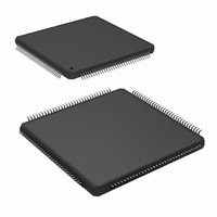
IC ADC 8BIT 3GSPS LP 128-LQFP
Manufacturer
National Semiconductor
Series
PowerWise®r
Datasheet
1.ADC083000CIYBNOPB.pdf
(40 pages)
Specifications of ADC083000CIYB/NOPB
Number Of Bits
8
Sampling Rate (per Second)
3G
Data Interface
Serial
Number Of Converters
2
Power Dissipation (max)
2.3W
Voltage Supply Source
Single Supply
Operating Temperature
-40°C ~ 85°C
Mounting Type
Surface Mount
Package / Case
128-LQFP Exposed Pad
Lead Free Status / RoHS Status
Lead free / RoHS Compliant
Other names
*ADC083000CIYB
*ADC083000CIYB/NOPB
ADC083000CIYB
*ADC083000CIYB/NOPB
ADC083000CIYB
Available stocks
Company
Part Number
Manufacturer
Quantity
Price
Company:
Part Number:
ADC083000CIYB/NOPB
Manufacturer:
IPS
Quantity:
2 300
Part Number:
ADC083000CIYB/NOPB
Manufacturer:
TI/德州仪器
Quantity:
20 000
www.national.com
1.4.1 Note Regarding Extended Mode Offset Correction
When using the Offset Adjust register, the following informa-
tion should be noted.
For offset values of +0000 0000 and -0000 0000, the actual
offset is not the same. By changing only the sign bit in this
case, an offset step in the digital output code of about 1/10th
of an LSB is experienced. This is shown more clearly in the
Figure below.
1.5 MULTIPLE ADC SYNCHRONIZATION
The ADC083000 has the capability to precisely reset its sam-
pling clock (CLK) to synchronize its output clock (DCLK) and
data with multiple ADCs in a system. This allows multiple AD-
Cs in a system to have their DCLK (and data) outputs transi-
tion at the same time with respect to the shared CLK input
that they all use for sampling.
The ADC083000 has been designed to accommodate sys-
tems which require a single-ended (LVCMOS) DCLK_RST or
a differential (LVDS) DCLK_RST.
Single-Ended (LVCMOS) DCLK_RST: The Power on Reset
state of DCLK_RST is to have single-ended DCLK_RST ac-
tivated. Bit 14, (DRE) in the Configuration Register is asserted
low, 0b. When not using singled-ended DCLK_RST, the input
should be grounded.
Differential (LVDS) DCLK_RST: Activated by asserting bit
14, (DRE) in the configuration register high, 1b. When the dif-
Note: The same bit pattern repeats when the test pattern sequence is concatenated.
FIGURE 10. Extended Mode Offset Behavior
Time
T10
T11
T0
T1
T2
T3
T4
T5
T6
T7
T8
T9
FEh
FEh
FEh
FEh
01h
01h
01h
01h
01h
01h
01h
Da
...
FDh
FDh
FDh
FDh
02h
02h
02h
02h
02h
02h
02h
Db
...
TABLE 5. Test Pattern by Output Port
20193230
FCh
FCh
FCh
FCh
03h
03h
03h
03h
03h
03h
03h
Dc
...
30
ferential DCLK_RST is not activated, the inputs should be
grounded. Differential DCLK_RST has an internal 100 ohm
termination resistor and should not be AC coupled.
The DCLK_RST signal must observe some timing require-
ments that are shown in Figure 5, Figure 6 and Figure 7 of the
Timing Diagrams. The DCLK_RST pulse must be of a mini-
mum width and its deassertion edge must observe setup and
hold times with respect to the CLK input rising edge. These
times are specified in the AC Electrical Characteristics Table.
The DCLK_RST signal can be asserted asynchronous to the
input clock. If DCLK_RST is asserted, the DCLK output is held
in a designated state. The state in which DCLK is held during
the reset period is determined by the mode of operation (SDR/
DDR) and the setting of the Output Edge configuration pin or
bit. (Refer to Figure 5, Figure 6 and Figure 7 for the DCLK
reset state conditions). Therefore, depending upon when the
DCLK_RST signal is asserted, there may be a narrow pulse
on the DCLK line during this reset event. When the
DCLK_RST signal is de-asserted in synchronization with the
CLK rising edge, the next CLK falling edge synchronizes the
DCLK output with those of other ADC083000s in the system.
The DCLK output is enabled again after a constant delay (rel-
ative to the input clock frequency) which is equal to the CLK
input to DCLK output delay (t
this delay characteristic in normal operation.
If the device is not programmed to allow DCLK to run contin-
uously, DCLK will become inactive during a calibration cycle.
Therefore, it is strongly recommended that DCLK only be
used as a data capture clock and not as a system clock.
The DCLK_RST pin should NOT be brought high while the
calibration process is running (while CalRun is high). Doing
so could cause a digital glitch in the digital circuitry, resulting
in corruption and invalidation of the calibration.
1.6 ADC TEST PATTERN
To aid in system debug, the ADC083000 has the capability of
providing a test pattern at the four output ports completely
independent of the input signal. The test pattern is selected
by setting bit-11 (TPO) in the Test Pattern Register (address
Fh). The test pattern will appear at the digital output about 10
DCLK cycles after the last write to the Test Pattern Register.
The ADC is disengaged and a test pattern generator is con-
nected to the outputs including OR. Each port is given a
unique 8-bit word, alternating between 1's and 0's as de-
scribed in theTable 5.
FBh
FBh
FBh
FBh
04h
04h
04h
04h
04h
04h
04h
Dd
...
OR
...
0
1
0
1
0
0
1
0
1
0
0
SD
). The device always exhibits
Pattern Sequence n+1
Pattern Sequence n+2
Pattern Sequence n
Comments


