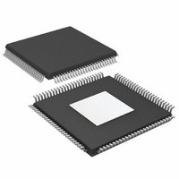
AD9430BSVZ-210 Analog Devices Inc, AD9430BSVZ-210 Datasheet - Page 23

AD9430BSVZ-210
Manufacturer Part Number
AD9430BSVZ-210
Description
IC ADC 12BIT 210MSPS 3.3V100TQFP
Manufacturer
Analog Devices Inc
Datasheet
1.AD9430BSVZ-210.pdf
(44 pages)
Specifications of AD9430BSVZ-210
Data Interface
Parallel
Number Of Bits
12
Sampling Rate (per Second)
210M
Number Of Converters
1
Power Dissipation (max)
1.7mW
Voltage Supply Source
Single Supply
Operating Temperature
-40°C ~ 85°C
Mounting Type
Surface Mount
Package / Case
100-TQFP Exposed Pad
Resolution (bits)
12bit
Sampling Rate
210MSPS
Input Channel Type
Differential
Supply Voltage Range - Digital
3V To 3.6V
Supply Current
390mA
Lead Free Status / RoHS Status
Lead free / RoHS Compliant
Available stocks
Company
Part Number
Manufacturer
Quantity
Price
Company:
Part Number:
AD9430BSVZ-210
Manufacturer:
AD
Quantity:
2 197
Part Number:
AD9430BSVZ-210
Manufacturer:
ADI/亚德诺
Quantity:
20 000
TERMINOLOGY
Analog Bandwidth
The analog input frequency at which the spectral power of the
fundamental frequency (as determined by the FFT analysis) is
reduced by 3 dB.
Aperture Delay
The delay between the 50% point of the rising edge of the
ENCODE command and the instant at which the analog input
is sampled.
Aperture Uncertainty (Jitter)
The sample-to-sample variation in aperture delay.
Crosstalk
Coupling onto one channel being driven by a low level
(–40 dBFS) signal when the adjacent interfering channel is
driven by a full-scale signal.
Differential Analog Input Resistance, Differential Analog
Input Capacitance, and Differential Analog Input Impedance
The real and complex impedances measured at each analog
input port. The resistance is measured statically and the
capacitance and differential input impedances are measured
with a network analyzer.
Differential Analog Input Voltage Range
The peak-to-peak differential voltage that must be applied to
the converter to generate a full-scale response. Peak differential
voltage is computed by observing the voltage on a single pin
and subtracting the voltage from the other pin, which is
180° out of phase. Peak-to-peak differential is computed by
rotating the input phase 180° and again taking the peak
measurement. The difference is then computed between both
peak measurements.
Differential Nonlinearity
The deviation of any code width from an ideal 1 LSB step.
Effective Number of Bits (ENOB)
Calculated from the measured SNR based on the equation
ENCODE Pulse Width/Duty Cycle
Pulse width high is the minimum amount of time the ENCODE
pulse (clock pulse) should be left in a Logic 1 state to achieve
rated performance; pulse width low is the minimum time the
ENCODE pulse should be left in a low state. See the timing
implications of changing t
a given clock rate, these specifications define an acceptable
ENCODE duty cycle.
ENOB
=
SNR
MEASURED
6.02
−
EH
1.76
in the Encode Input section. At
dB
Rev. E | Page 23 of 44
Full-Scale Input Power
Expressed in dBm. Computed using the following equation:
Gain Error
The difference between the measured and ideal full-scale input
voltage range of the ADC.
Harmonic Distortion, Second
The ratio of the rms signal amplitude to the rms value of the
second harmonic component, reported in dBc.
Harmonic Distortion, Third
The ratio of the rms signal amplitude to the rms value of the
third harmonic component, reported in dBc.
Integral Nonlinearity
The deviation of the transfer function from a reference line
measured in fractions of 1 LSB using a best straight line
determined by a least square curve fit.
Minimum Conversion Rate
The ENCODE rate at which the SNR of the lowest analog
signal frequency drops by no more than 3 dB below the
guaranteed limit.
Maximum Conversion Rate
The ENCODE rate at which parametric testing is performed.
Output Propagation Delay
The delay between a differential crossing of CLK+ and CLK– and
the time when all output data bits are within valid logic levels.
Noise (for Any Range Within the ADC)
Calculated as follows:
where:
Z is the input impedance.
FS is the full scale of the device for the frequency in question.
SNR is the value of the particular input level.
Signal is the signal level within the ADC, reported in dB below
full scale. This value includes input levels both thermal and
quantization noise.
Power
V
NOISE
FULL
=
SCALE
Z
×
. 0
=
001
10
×
log
10
⎛
⎜
⎜
⎜
⎜
⎝
⎛
⎜
⎝
V
FS
2
dBM
FULL
Z
. 0
INPUT
001
−
SCALE
SNR
rms
10
dBc
⎞
⎟
⎟
⎟
⎟
⎠
−
Signal
dBFS
AD9430
⎞
⎟
⎠


