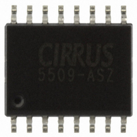
CS5509-ASZ Cirrus Logic Inc, CS5509-ASZ Datasheet - Page 12

CS5509-ASZ
Manufacturer Part Number
CS5509-ASZ
Description
IC ADC 16BIT SGNL SUPP 16-SOIC
Manufacturer
Cirrus Logic Inc
Datasheet
1.CS5509-ASZ.pdf
(24 pages)
Specifications of CS5509-ASZ
Number Of Converters
1
Package / Case
16-SOIC (0.300", 7.50mm Width)
Number Of Bits
16
Sampling Rate (per Second)
200
Data Interface
Serial
Power Dissipation (max)
2.25mW
Voltage Supply Source
Analog and Digital
Operating Temperature
-40°C ~ 85°C
Mounting Type
Surface Mount
Number Of Adc Inputs
1
Architecture
Delta-Sigma
Conversion Rate
20 SPs
Resolution
16 bit
Input Type
Voltage
Interface Type
Serial
Voltage Reference
1.2 V
Supply Voltage (max)
5 V
Supply Voltage (min)
3.3 V
Maximum Power Dissipation
2.25 mW
Maximum Operating Temperature
+ 85 C
Mounting Style
SMD/SMT
Input Voltage
3.3 V to 5 V
Minimum Operating Temperature
- 40 C
Lead Free Status / RoHS Status
Lead free / RoHS Compliant
Lead Free Status / RoHS Status
Lead free / RoHS Compliant, Lead free / RoHS Compliant
Other names
598-1100-5
Available stocks
Company
Part Number
Manufacturer
Quantity
Price
Company:
Part Number:
CS5509-ASZ
Manufacturer:
CIRRUS
Quantity:
44
Part Number:
CS5509-ASZ
Manufacturer:
CIRRUS
Quantity:
20 000
in the reference without recalibration, accommo-
dating ratiometric applications.
Analog Input Range
The analog input range is set by the magnitude of
the voltage between the VREF+ and VREF- pins.
In unipolar mode the input range will equal the
magnitude of the voltage reference. In bipolar
mode the input voltage range will equate to plus
and minus the magnitude of the voltage reference.
While the voltage reference can be as great as 3.6
volts, its common mode voltage can be any value as
long as the reference inputs VREF+ and VREF-
stay within the supply voltages VA+ and GND.
The differential input voltage can also have any
common mode value as long as the maximum sig-
nal magnitude stays within the supply voltages.
The A/D converter is intended to measure dc or low
frequency inputs. It is designed to yield accurate
conversions even with noise exceeding the input
voltage range as long as the spectral components of
this noise will be filtered out by the digital filter.
For example, with a 3.0 volt reference in unipolar
mode, the converter will accurately convert an in-
put dc signal up to 3.0volts with up to 15% over-
range for 60Hz noise. A 3.0volt dc signal could
have a 60Hz component which is 0.5volts above
the maximum input of 3.0 (3.5 volts peak; 3.0 volts
dc plus 0.5 volts peak noise) and still accurately
convert the input signal (XIN = 32.768 kHz). This
assumes that the signal plus noise amplitude stays
within the supply voltages.
The CS5509 converters output data in binary for-
mat when converting unipolar signals and in offset
binary format when converting bipolar signals. Ta-
ble 1 outlines the output coding for both unipolar
and bipolar measurement modes.
Converter Performance
The CS5509 A/D converter has excellent linearity
performance. Calibration minimizes the errors in
12
offset and gain. The CS5509 device has no missing
code performance to 16-bits. Figure4 illustrates the
DNL of the CS5509. The converter achieves Com-
mon Mode Rejection (CMR) at dc of 105dB typi-
cal, and CMR at 50 and 60Hz of 120dB typical.
The CS5509 can experience some drift as tempera-
ture changes. The CS5509 uses chopper-stabilized
techniques to minimize drift. Measurement errors
due to offset or gain drift can be eliminated at any
time by recalibrating the converter.
Analog Input Impedance Considerations
The analog input of the CS5509 can be modeled as
illustrated in Figure 5. Capacitors (15 pF each) are
used to dynamically sample each of the inputs
(AIN+ and AIN-). Every half XIN cycle the switch
alternately connects the capacitor to the output of
the buffer and then directly to the AIN pin. When-
ever the sample capacitor is switched from the out-
put of the buffer to the AIN pin, a small packet of
charge (a dynamic demand of current) is required
from the input source to settle the voltage of the
sample capacitor to its final value. The voltage on
the output of the buffer may differ up to 100 mV
from the actual input voltage due to the offset volt-
age of the buffer. Timing allows one half of a XIN
clock cycle for the voltage on the sample capacitor
to settle to its final value.
Note: Table excludes common mode voltage on the
> (VREF - 1.5 LSB)
VREF/2 - 0.5 LSB
VREF - 1.5 LSB
Unipolar Input
< (+0.5 LSB)
+0.5 LSB
Voltage
signal and reference inputs.
Table 1. Output Coding
Output
Codes
--------------- -
FFFE
FFFF
-------------- -
7FFF
FFFF
8000
0001
------------ -
0000
0000
< (-VREF + 0.5 LSB)
> (VREF - 1.5 LSB)
-VREF + 0.5 LSB
VREF - 1.5 LSB
Bipolar Input
-0.5 LSB
Voltage
CS5509
DS125F3


