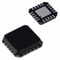
AD7699BCPZ Analog Devices Inc, AD7699BCPZ Datasheet - Page 4

AD7699BCPZ
Manufacturer Part Number
AD7699BCPZ
Description
IC ADC 8CH 16BIT 500KSPS 20LFCSP
Manufacturer
Analog Devices Inc
Datasheet
1.AD7699BCPZ.pdf
(28 pages)
Specifications of AD7699BCPZ
Data Interface
DSP, MICROWIRE™, QSPI™, Serial, SPI™
Number Of Bits
16
Sampling Rate (per Second)
500k
Number Of Converters
1
Power Dissipation (max)
32mW
Voltage Supply Source
Single Supply
Operating Temperature
-40°C ~ 85°C
Mounting Type
Surface Mount
Package / Case
20-VFQFN, CSP Exposed Pad
Resolution (bits)
16bit
Sampling Rate
500kSPS
Input Channel Type
Pseudo Differential, Single Ended
Supply Voltage Range - Analog
4.5V To 5.5V
Lead Free Status / RoHS Status
Lead free / RoHS Compliant
Available stocks
Company
Part Number
Manufacturer
Quantity
Price
Company:
Part Number:
AD7699BCPZ
Manufacturer:
ADI
Quantity:
490
Part Number:
AD7699BCPZ
Manufacturer:
ADI/亚德诺
Quantity:
20 000
AD7699
Parameter
INTERNAL REFERENCE
EXTERNAL REFERENCE
TEMPERATURE SENSOR
DIGITAL INPUTS
DIGITAL OUTPUTS
POWER SUPPLIES
TEMPERATURE RANGE
1
2
3
4
5
6
7
8
9
10
11
12
See the Analog Inputs section.
The bandwidth is set with the configuration register.
LSB means least significant bit. With the 5 V input range, one LSB = 76.3 µV.
See the Terminology section. These specifications include full temperature range variation but not the error contribution from the reference.
All specifications expressed in decibels are referred to a full-scale input FSR and tested with an input signal at 0.5 dB below full scale, unless otherwise specified.
This is the output from the internal band gap.
The output voltage is internal and present on a dedicated multiplexer input.
Unipolar mode: serial 16-bit straight binary.
Conversion results available immediately after completed conversion.
Bipolar mode: serial 16-bit twos complement.
With all digital inputs forced to VIO or GND as required.
During acquisition phase.
Contact an Analog Devices, Inc., sales representative for the extended temperature range.
Temperature Sensitivity
VDD
VIO
REF Output Voltage
REFIN Output Voltage
REF Output Current
Temperature Drift
Line Regulation
Long-Term Drift
Turn-On Settling Time
Voltage Range
Current Drain
Output Voltage
Logic Levels
Data Format
Pipeline Delay
V
V
Standby Current
Power Dissipation
Energy per Conversion
Specified Performance
OL
OH
V
V
I
I
IL
IH
IL
IH
8
9
7
10, 11
12
6
Conditions/Comments
@ 25°C
@ 25°C
VDD = 5 V ± 5%
1000 hours
CREF = 10 µF
REF input
REFIN input (buffered)
500 kSPS, REF = 5 V
@ 25°C
I
I
Specified performance
Specified performance
VDD and VIO = 5 V, @ 25°C
VDD = 5 V, 100 kSPS throughput
VDD = 5 V, 500 kSPS throughput
VDD = 5 V, 500 kSPS throughput with internal reference
T
SINK
SOURCE
MIN
= +500 µA
to T
= −500 µA
MAX
Rev. 0 | Page 4 of 28
Min
4.086
0.5
0.5
−0.3
0.7 × VIO
−1
−1
VIO − 0.3
4.5
1.8
−40
Typ
4.096
2.3
±300
±10
±15
50
5
100
283
1
50
5.2
26
28
52
Max
4.106
VDD + 0.3
VDD − 0.2
+0.3 × VIO
VIO + 0.3
+1
+1
0.4
5.5
VDD + 0.3
29
32
+85
Unit
V
V
µA
ppm/°C
ppm/V
ppm
ms
V
V
µA
mV
mV/°C
V
V
µA
µA
V
V
V
V
nA
µW
mW
mW
nJ
°C


