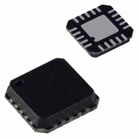
AD7699BCPZ Analog Devices Inc, AD7699BCPZ Datasheet - Page 18

AD7699BCPZ
Manufacturer Part Number
AD7699BCPZ
Description
IC ADC 8CH 16BIT 500KSPS 20LFCSP
Manufacturer
Analog Devices Inc
Datasheet
1.AD7699BCPZ.pdf
(28 pages)
Specifications of AD7699BCPZ
Data Interface
DSP, MICROWIRE™, QSPI™, Serial, SPI™
Number Of Bits
16
Sampling Rate (per Second)
500k
Number Of Converters
1
Power Dissipation (max)
32mW
Voltage Supply Source
Single Supply
Operating Temperature
-40°C ~ 85°C
Mounting Type
Surface Mount
Package / Case
20-VFQFN, CSP Exposed Pad
Resolution (bits)
16bit
Sampling Rate
500kSPS
Input Channel Type
Pseudo Differential, Single Ended
Supply Voltage Range - Analog
4.5V To 5.5V
Lead Free Status / RoHS Status
Lead free / RoHS Compliant
Available stocks
Company
Part Number
Manufacturer
Quantity
Price
Company:
Part Number:
AD7699BCPZ
Manufacturer:
ADI
Quantity:
490
Part Number:
AD7699BCPZ
Manufacturer:
ADI/亚德诺
Quantity:
20 000
AD7699
DRIVER AMPLIFIER CHOICE
Although the AD7699 is easy to drive, the driver amplifier must
meet the following requirements:
•
•
•
Table 7. Recommended Driver Amplifiers
Amplifier
ADA4841-x
AD8655
AD8021
AD8022
OP184
AD8605,
VOLTAGE REFERENCE OUTPUT/INPUT
The AD7699 allows the choice of a very low temperature drift
internal voltage reference, an external reference, or an external
buffered reference.
The internal reference of the AD7699 provides excellent
performance and can be used in almost all applications. There
are five possible choices of voltage reference schemes briefly
The noise generated by the driver amplifier must be kept
as low as possible to preserve the SNR and transition noise
performance of the AD7699. Note that the AD7699 has a
noise much lower than most of the other 16-bit ADCs and,
therefore, can be driven by a noisier amplifier to meet a given
system noise specification. The noise from the amplifier is
filtered by the AD7699 analog input circuit low-pass filter
made by R
Because the typical noise of the AD7699 is 35 µV rms (with
V
where:
f
(14.7 MHz in full BW or 670 kHz in ¼ BW) or the cutoff
frequency of an input filter, if one is used.
N is the noise gain of the amplifier (for example, 1 in buffer
configuration).
e
nV/√Hz.
For ac applications, the driver should have a THD perfor-
mance commensurate with the AD7699. Figure 12 shows
THD vs. frequency for the AD7699.
For multichannel, multiplexed applications on each input
or input pair, the driver amplifier and the AD7699 analog
input circuit must settle a full-scale step onto the capacitor
array at a 16-bit level (0.0015%). In amplifier data sheets,
settling at 0.1% to 0.01% is more commonly specified. This
may differ significantly from the settling time at a 16-bit
level and should be verified prior to driver selection.
SNR
−3dB
N
REF
is the equivalent input noise voltage of the op amp, in
AD8615
is the input bandwidth in megahertz of the AD7699
= 5 V), the SNR degradation due to the amplifier is
LOSS
=
IN
20
and C
log
Typical Application
Very low noise, small, and low power
5 V single supply, low noise
Very low noise and high frequency
Low noise and high frequency
Low power, low noise, and low frequency
5 V single supply, low power
IN
or by an external filter, if one is used.
35
2
+
π
2
35
f
−
3dB
(
Ne
N
)
2
Rev. 0 | Page 18 of 28
described in Table 8 with more details in each of the following
sections.
Internal Reference/Temperature Sensor
The internal reference can be set for a 4.096 V output as
detailed in Table 8. With the internal reference enabled, the
band gap voltage is also present on the REFIN pin, which
requires an external 0.1 μF capacitor. Because the current
output of REFIN is limited, it can be used as a source if followed
by a suitable buffer, such as the AD8605.
Enabling the reference also enables the internal temperature
sensor, which measures the internal temperature of the AD7699
and is thus useful for performing a system calibration. Note
that, when using the temperature sensor, the output is straight
binary referenced from the AD7699 GND pin.
The internal reference is temperature-compensated to within
15 mV. The reference is trimmed to provide a typical drift of
3 ppm/°C.
External Reference and Internal Buffer
For improved drift performance, an external reference can be
used with the internal buffer. The external reference is connected
to REFIN, and the output is produced on the REF pin. An
external reference can be used with the internal buffer with or
without the temperature sensor enabled. Refer to Table 8 for
register details. With the buffer enabled, the gain is unity and is
limited to an input/output of 4.096 V.
The internal reference buffer is useful in multiconverter applica-
tions because a buffer is typically required in these applications. In
addition, a low power reference can be used because the internal
buffer provides the necessary performance to drive the SAR
architecture of the AD7699.
External Reference
In any of the five voltage reference schemes, an external refer-
ence can be connected directly on the REF pin because the output
impedance of REF is >5 kΩ. To reduce power consumption, the
reference and buffer can be powered down independently or
together for the lowest power consumption. However, for applica-
tions requiring the use of the temperature sensor, the reference
must be active. Refer to Table 8 for register details. For improved
drift performance, an external reference such as the
ADR44x
Reference Decoupling
Whether using an internal or external reference, the AD7699
voltage reference output/input, REF, has a dynamic input
impedance and should therefore be driven by a low impedance
source with efficient decoupling between the REF and GND
pins. This decoupling depends on the choice of the voltage
reference but usually consists of a low ESR capacitor connected
to REF and GND with minimum parasitic inductance. A 10 µF
(X5R, 1206 size) ceramic chip capacitor is appropriate when
using the internal reference, the ADR43x/ADR44x external
is recommended.
ADR43x
or


