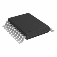
AD7866ARUZ Analog Devices Inc, AD7866ARUZ Datasheet - Page 4

AD7866ARUZ
Manufacturer Part Number
AD7866ARUZ
Description
IC ADC 12BIT 2CH DUAL 20-TSSOP
Manufacturer
Analog Devices Inc
Datasheet
1.AD7866ARU-REEL.pdf
(24 pages)
Specifications of AD7866ARUZ
Data Interface
DSP, MICROWIRE™, QSPI™, Serial, SPI™
Number Of Bits
12
Sampling Rate (per Second)
1M
Number Of Converters
2
Power Dissipation (max)
24mW
Voltage Supply Source
Analog and Digital
Operating Temperature
-40°C ~ 125°C
Mounting Type
Surface Mount
Package / Case
20-TSSOP (0.173", 4.40mm Width)
Resolution (bits)
12bit
Input Channel Type
Single Ended
Supply Voltage Range - Analogue
2.7V To 5.25V
Supply Voltage Range - Digital
2.7V To 5.25V
Supply
RoHS Compliant
Sampling Rate
1MSPS
Rohs Compliant
Yes
Number Of Elements
2
Resolution
12Bit
Architecture
SAR
Sample Rate
1MSPS
Input Polarity
Unipolar
Input Type
Voltage
Rated Input Volt
2.5/5V
Differential Input
No
Power Supply Requirement
Analog and Digital
Single Supply Voltage (typ)
3/5V
Single Supply Voltage (min)
2.7V
Single Supply Voltage (max)
5.25V
Dual Supply Voltage (typ)
Not RequiredV
Dual Supply Voltage (min)
Not RequiredV
Dual Supply Voltage (max)
Not RequiredV
Power Dissipation
24mW
Differential Linearity Error
-0.95LSB/1.25LSB
Integral Nonlinearity Error
±1.5LSB
Operating Temp Range
-40C to 125C
Operating Temperature Classification
Automotive
Mounting
Surface Mount
Pin Count
20
Package Type
TSSOP
Input Signal Type
Single-Ended
Lead Free Status / RoHS Status
Lead free / RoHS Compliant
For Use With
EVAL-AD7866CBZ - BOARD EVALUATION AD7866
Lead Free Status / Rohs Status
Compliant
Available stocks
Company
Part Number
Manufacturer
Quantity
Price
Part Number:
AD7866ARUZ
Manufacturer:
ADI/亚德诺
Quantity:
20 000
Part Number:
AD7866ARUZ-REEL7
Manufacturer:
ADI/亚德诺
Quantity:
20 000
AD7866
TIMING SPECIFICATIONS
Parameter
f
t
t
t
t
t
t
t
t
t
t
NOTES
1
2
3
4
Specifications subject to change without notice.
SCLK
CONVERT
QUIET
2
3
4
5
6
7
8
9
Sample tested at 25°C to ensure compliance. All input signals are specified with t
Mark/Space ratio for the CLK input is 40/60 to 60/40.
Measured with the load circuit of Figure 1 and defined as the time required for the output to cross 0.8 V or 2.0 V.
t
lated back to remove the effects of charging or discharging the 50 pF capacitor. This means that the times t
bus relinquish times of the part and are independent of the bus loading.
8,
3
3
4
4
t
9
are derived from the measured time taken by the data outputs to change 0.5 V when loaded with the circuit of Figure 1. The measured number is then extrapo-
2
Limit at
T
10
20
16
800
50
10
25
40
0.4 t
0.4 t
10
25
10
50
MIN
SCLK
SCLK
, T
t
SCLK
MAX
Figure 1. Load Circuit for Digital Output Timing Specifications
Unit
kHz min
MHz max
ns max
ns max
ns max
ns min
ns max
ns max
ns min
ns min
ns min
ns max
ns min
ns max
1
(V
DD
= 2.7 V to 5.25 V, V
OUTPUT
PIN
TO
50pF
Description
t
f
Minimum Time between End of Serial Read and Next Falling Edge of CS
CS to SCLK Setup Time
Delay from CS until D
Data Access Time after SCLK Falling Edge. V
V
SCLK Low Pulsewidth
SCLK High Pulsewidth
SCLK to Data Valid Hold Time
CS Rising Edge to D
SCLK Falling Edge to D
SCLK Falling Edge to D
C
SCLK
SCLK
L
DRIVE
200 A
200 A
= 20 MHz
= 1/f
DRIVE
< 3 V, C
–4–
= 2.7 V to 5.25 V, V
SCLK
R
= t
I
I
F
OL
OH
= 5 ns (10% to 90% of V
L
= 25 pF
OUT
OUT
1.6V
A, D
OUT
OUT
A and D
REF
A, D
A, D
OUT
= 2.5 V; T
8
and t
B, High Impedance
OUT
OUT
OUT
DRIVE
9
B, High Impedance
B, High Impedance
quoted in the timing characteristics are the true
B Three-State Disabled
) and timed from a voltage level of 1.6 V.
A
= T
MIN
DRIVE
to T
MAX
, unless otherwise noted.)
3 V, C
L
= 50 pF;
REV. A


