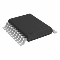
AD7866ARUZ Analog Devices Inc, AD7866ARUZ Datasheet - Page 2

AD7866ARUZ
Manufacturer Part Number
AD7866ARUZ
Description
IC ADC 12BIT 2CH DUAL 20-TSSOP
Manufacturer
Analog Devices Inc
Datasheet
1.AD7866ARU-REEL.pdf
(24 pages)
Specifications of AD7866ARUZ
Data Interface
DSP, MICROWIRE™, QSPI™, Serial, SPI™
Number Of Bits
12
Sampling Rate (per Second)
1M
Number Of Converters
2
Power Dissipation (max)
24mW
Voltage Supply Source
Analog and Digital
Operating Temperature
-40°C ~ 125°C
Mounting Type
Surface Mount
Package / Case
20-TSSOP (0.173", 4.40mm Width)
Resolution (bits)
12bit
Input Channel Type
Single Ended
Supply Voltage Range - Analogue
2.7V To 5.25V
Supply Voltage Range - Digital
2.7V To 5.25V
Supply
RoHS Compliant
Sampling Rate
1MSPS
Rohs Compliant
Yes
Number Of Elements
2
Resolution
12Bit
Architecture
SAR
Sample Rate
1MSPS
Input Polarity
Unipolar
Input Type
Voltage
Rated Input Volt
2.5/5V
Differential Input
No
Power Supply Requirement
Analog and Digital
Single Supply Voltage (typ)
3/5V
Single Supply Voltage (min)
2.7V
Single Supply Voltage (max)
5.25V
Dual Supply Voltage (typ)
Not RequiredV
Dual Supply Voltage (min)
Not RequiredV
Dual Supply Voltage (max)
Not RequiredV
Power Dissipation
24mW
Differential Linearity Error
-0.95LSB/1.25LSB
Integral Nonlinearity Error
±1.5LSB
Operating Temp Range
-40C to 125C
Operating Temperature Classification
Automotive
Mounting
Surface Mount
Pin Count
20
Package Type
TSSOP
Input Signal Type
Single-Ended
Lead Free Status / RoHS Status
Lead free / RoHS Compliant
For Use With
EVAL-AD7866CBZ - BOARD EVALUATION AD7866
Lead Free Status / Rohs Status
Compliant
Available stocks
Company
Part Number
Manufacturer
Quantity
Price
Part Number:
AD7866ARUZ
Manufacturer:
ADI/亚德诺
Quantity:
20 000
Part Number:
AD7866ARUZ-REEL7
Manufacturer:
ADI/亚德诺
Quantity:
20 000
AD7866–SPECIFICATIONS
Parameter
DYNAMIC PERFORMANCE
SAMPLE AND HOLD
DC ACCURACY
ANALOG INPUT
REFERENCE INPUT/OUTPUT
LOGIC INPUTS
LOGIC OUTPUTS
Signal to Noise + Distortion (SINAD)
Total Harmonic Distortion (THD)
Peak Harmonic or Spurious Noise (SFDR)
Intermodulation Distortion (IMD)
Aperture Delay
Aperture Jitter
Aperture Delay Matching
Full Power Bandwidth
Resolution
Integral Nonlinearity
Differential Nonlinearity
0 V to V
2
Input Voltage Ranges
DC Leakage Current
Input Capacitance
Reference Input Voltage
Reference Input Voltage Range
DC Leakage Current
Input Capacitance
Reference Output Voltage
V
Reference Temperature Coefficient
REF OUT Error (T
Input High Voltage, V
Input Low Voltage, V
Input Current, I
Input Capacitance, C
Output High Voltage, V
Output Low Voltage, V
Floating-State Leakage Current
Floating-State Output Capacitance
Output Coding
REF
Second Order Terms
Third Order Terms
Channel-to-Channel Isolation
Offset Error
Offset Error Match
Gain Error
Gain Error Match
Positive Gain Error
Zero Code Error
Zero Code Error Match
Negative Gain Error
V
Output Impedance
REF
REF
Input Range
Input Range
3
3
IN
MIN
IN
INL
INH
3
OL
to T
OH
6
3
5
MAX
4
)
2
2
3
2
2
A Version
68
–75
–76
–88
–88
–88
10
50
200
12
2
12
± 1.5
–0.95/+1.25
± 8
± 1.2
± 2.5
± 0.2
± 2.5
± 8
± 0.2
± 2.5
0 to V
0 to 2
± 500
1
30
10
2.5
2/3
± 30
± 160
20
2.45/2.55
25
45
50
± 15
0.7 V
0.3 V
± 1
10
V
0.4
± 1
10
Straight (Natural) Binary
Twos Complement
DRIVE
DRIVE
DRIVE
(T
External on D
REF
– 0.2
A
= T
V
REF
1
MIN
to T
B Version
68
–75
–76
–88
–88
–88
10
50
200
12
2
12
± 1
± 1.5
–0.95/+1.25
± 8
± 1.2
± 2.5
± 0.2
± 2.5
± 8
± 0.2
± 2.5
0 to V
0 to 2
± 500
1
30
10
2.5
2/3
± 30
± 160
20
2.45/2.55
25
45
50
± 15
0.7 V
0.3 V
± 1
10
V
0.4
± 1
10
DRIVE
–2–
CAP
MAX
A and D
DRIVE
DRIVE
, V
REF
– 0.2
DD
V
= 2.7 V to 5.25 V, V
REF
1
CAP
Unit
dB min
dB max
dB max
dB typ
dB typ
ns max
ps typ
ps max
MHz typ
MHz typ
Bits
LSB max
LSB max
LSB max
LSB max
LSB typ
LSB max
LSB typ
LSB max
LSB max
LSB typ
LSB max
V
V
nA max
µA max
pF typ
pF typ
V min/V max REF SELECT Pin Tied High
µA max
µA max
pF typ
V min/V max
Ω typ
Ω typ
mV typ
V min
V max
µA max
pF max
V min
V max
µA max
pF max
B, f
dB typ
V
ppm/°C typ
SCLK
= 20 MHz, unless otherwise noted.)
DRIVE
Test Conditions/Comments
f
f
f
@ 3 dB
@ 0.1 dB
B Grade, 0 V to V
0 V to 2
Guaranteed No Missed Codes to 12 Bits
Straight Binary Output Coding
–V
Twos Complement Output Coding
RANGE Pin Low upon CS Falling Edge
RANGE Pin High upon CS Falling Edge
T
85 C < T
When in Track
When in Hold
± 1% for Specified Performance
V
D
V
V
Typically 15 nA, V
I
I
V
Selectable with Either Input Range
IN
IN
IN
SOURCE
SINK
A
REF
DD
DD
DD
CAP
REF
= 300 kHz Sine Wave, f
= 2.7 V to 5.25 V, Reference = 2.5 V
= 300 kHz Sine Wave, f
= 300 kHz Sine Wave, f
= –40 C to +85 C
= 5 V
= 3 V
= 2.7 V to 5.25 V
Pin
A, D
= 200 µA
to +V
= 200 µA
A
CAP
≤
V
REF
REF
B Pins
125 C
REF
Biased about V
Range; ± 0.5 LSB typ
IN
Range Only; ±0.5 LSB typ
= 0 V or V
S
S
S
= 1 MSPS
= 1 MSPS
= 1 MSPS
REF
DRIVE
REV. A
with


