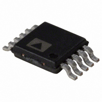
AD7992BRMZ-1 Analog Devices Inc, AD7992BRMZ-1 Datasheet - Page 27

AD7992BRMZ-1
Manufacturer Part Number
AD7992BRMZ-1
Description
IC ADC 12BIT 2CHAN I2C 10-MSOP
Manufacturer
Analog Devices Inc
Datasheet
1.AD7992BRMZ-1.pdf
(28 pages)
Specifications of AD7992BRMZ-1
Data Interface
I²C, Serial
Operating Temperature
-40°C ~ 125°C
Number Of Bits
12
Sampling Rate (per Second)
79k
Number Of Converters
1
Power Dissipation (max)
2.2mW
Voltage Supply Source
Single Supply
Mounting Type
Surface Mount
Package / Case
10-TFSOP (0.118", 3.00mm Width)
Resolution (bits)
12bit
Input Channel Type
Single Ended
Supply Voltage Range - Analogue
2.7V To 5.5V
Supply Current
1.4mA
No. Of Pins
10
Sampling Rate
188kSPS
Rohs Compliant
Yes
Lead Free Status / RoHS Status
Lead free / RoHS Compliant
For Use With
EVAL-AD7992CB - BOARD EVALUATION FOR AD7992
Lead Free Status / RoHS Status
Lead free / RoHS Compliant
Available stocks
Company
Part Number
Manufacturer
Quantity
Price
Part Number:
AD7992BRMZ-1
Manufacturer:
ADI/亚德诺
Quantity:
20 000
MODE 3—AUTOMATIC CYCLE MODE
An automatic conversion cycle can be selected and enabled by
writing a value to the cycle timer register. A conversion cycle
interval can be set up on the AD7992 by programming the
relevant bits in the 8-bit cycle timer register, as decoded in
Table 23. Only the 3 LSBs are used; the 5 MSBs should contain
0s (see the Sample Delay and Bit Trial Delay section). When the
3 LSBs of the register are programmed with any configuration
other than all 0s, a conversion takes place every X ms; the cycle
interval, X, depends on the configuration of these three bits in
the cycle timer register. There are seven different cycle time
intervals to choose from, as shown in Table 23. Once the
conversion has taken place, the part powers down again until
the next conversion occurs. To exit this mode of operation, the
user must program the 3 LSBs of the cycle timer register to
contain all 0s. For cycle interval options, see Table 23.
SDA
SCL
SDA
SCL
Sr
S
1
1
7-BIT ADDRESS
7-BIT ADDRESS
W A
8
R A
ACK BY
ACK BY
AD7992
AD7992
9
9
1
1
COMMAND/ADDRESS
FIRST DATA BYTE
POINT BYTE
(MSBs)
Figure 33. Mode 2 Sequence Operation
MASTER
ACK BY
RESULT FROM CH1
ACK BY
AD7992
A
A
9
9
Rev. 0 | Page 27 of 28
SECOND DATA BYTE
(LSBs)
To select a channel(s) for operation in cycle mode, set the
corresponding channel bit(s), D5 to D4, of the configuration
register. If more than one channel bit is set in the configuration
register, the ADC automatically cycles through the channel
sequence, starting with the lowest channel. Once the sequence
is complete, the ADC starts converting on the lowest channel
again, continuing to loop through the sequence until the cycle
timer register contents are set to all 0s. This mode is useful for
monitoring signals, such as battery voltage and temperature,
alerting only when the limits are violated.
MASTER
ACK BY
A
9
FIRST DATA BYTE
(MSBs)
RESULT FROM CH2
MASTER
ACK BY
A
9
SECOND DATA BYTE
(LSBs)
AD7992
A/A
9


