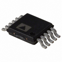
AD7992BRMZ-1 Analog Devices Inc, AD7992BRMZ-1 Datasheet - Page 17

AD7992BRMZ-1
Manufacturer Part Number
AD7992BRMZ-1
Description
IC ADC 12BIT 2CHAN I2C 10-MSOP
Manufacturer
Analog Devices Inc
Datasheet
1.AD7992BRMZ-1.pdf
(28 pages)
Specifications of AD7992BRMZ-1
Data Interface
I²C, Serial
Operating Temperature
-40°C ~ 125°C
Number Of Bits
12
Sampling Rate (per Second)
79k
Number Of Converters
1
Power Dissipation (max)
2.2mW
Voltage Supply Source
Single Supply
Mounting Type
Surface Mount
Package / Case
10-TFSOP (0.118", 3.00mm Width)
Resolution (bits)
12bit
Input Channel Type
Single Ended
Supply Voltage Range - Analogue
2.7V To 5.5V
Supply Current
1.4mA
No. Of Pins
10
Sampling Rate
188kSPS
Rohs Compliant
Yes
Lead Free Status / RoHS Status
Lead free / RoHS Compliant
For Use With
EVAL-AD7992CB - BOARD EVALUATION FOR AD7992
Lead Free Status / RoHS Status
Lead free / RoHS Compliant
Available stocks
Company
Part Number
Manufacturer
Quantity
Price
Part Number:
AD7992BRMZ-1
Manufacturer:
ADI/亚德诺
Quantity:
20 000
CONFIGURATION REGISTER
The configuration register is a 8-bit, read/write register that is used to set the operating modes of the AD7992. The MSB of the register is
unused and is a don’t care bit. The bit functions of the configuration register are outlined in Table 9. A single-byte write is necessary when
writing to the configuration register.
Table 9. Configuration Register Bit Function Descriptions and Default Settings at Power-Up
D7
DONTC
0
Bit
D7
D6
D5, D4
D3
D2
D1
D0
Table 10. Channel and Reference Selection
D6
Single/Dual
0
0
1
0
0
Table 11. ALERT/BUSY Function
D2
0
0
1
1
D6
Single/Dual
0
Mnemonic
DONTC
Single/Dual
CH2, CH1
FLTR
ALERT EN
BUSY/ALERT
BUSY/ALERT
POLARITY
D5
CH2
0
0
0
1
1
D1
0
1
0
1
D5
CH2
0
Comment
Don’t care bit.
The value written to this bit determines the functionality of the V
conversions. When this bit is 1, the pin takes on its reference input function, REF
channel part with the reference being taken from the REF
conversion, the reference can also be taken from the supply voltage by setting D6 to 0. When this bit is a 0, the
V
reference being taken from the supply voltage. See Table 10.
These two channel address bits select which analog input channel is to be converted. A 1 in any of Bits D5 or D4
selects a channel for conversion. If more than one channel bit is set (with D6 = 0), the alternating channel
sequence is used. Table 10 shows how these two channel address bits are decoded. If D5 is selected, the part
operates in dual-channel mode, with the reference for the ADC being taken from the supply voltage (D6 set to 0
for dual-channel mode).
The value written to this bit of the control register determines whether the filtering on SDA and SCL is enabled or
is bypassed. If this bit is a 1, the the filtering is enabled; if it is a 0, the filtering is bypassed.
The hardware ALERT function is enabled if this bit is set to 1 and disabled if this bit is set to 0. This bit is used in
conjunction with the BUSY/ALERT bit to determine if the ALERT/BUSY pin acts as an ALERT or a BUSY output
(see Table 11).
This bit is used in conjunction with the ALERT EN bit to determine if the ALERT/BUSY pin acts as an ALERT or
BUSY output (see Table 11), and if configured as an ALERT output pin, if it is to be reset.
This bit determines the active polarity of the ALERT/BUSY pin regardless of whether it is configured as an ALERT
or BUSY output. It is active low if this bit is set to 0 and active high if set to 1.
IN
2/REF
D4
CH1
0
1
1
0
1
ALERT/BUSY Pin Configuration
Pin does not provide any interrupt signal.
Pin configured as a BUSY output.
Pin configured as an ALERT output.
Resets the ALERT output pin, the Alert_Flag bit in the conversion result register, and the entire alert status
register (if any is active). If 1/1 is written to Bits D2/D1 in the configuration register to reset the ALERT pin, the
Alert_Flag bit, and the alert status register, the contents of the configuration register read 1/0 for D2/D1,
respectively, if read back.
IN
D4
CH1
0
pin becomes a second analog input pin, V
Analog Input Channel
No conversion
Convert on V
Convert on V
Convert on V
Sequence between Channel 1 and Channel 2, beginning with Channel 1 (reference from V
D3
FLTR
1
IN
IN
IN
D2
ALERT EN
0
1 (reference from V
1 (reference from REF
2 (reference from V
Rev. 0 | Page 17 of 28
DD
DD
D1
BUSY/ALERT
0
IN
)
)
2, making the AD7992 a dual-channel part with the
IN
)
IN
pin. However, when only Channel 1 is selected for a
IN
2/REF
IN
pin and the reference source for the
D0
ALERT/BUSY POLARITY
0
IN
, making the AD7992 a single-
AD7992
DD
)


