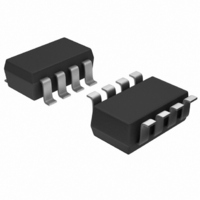
AD7999YRJZ-1500RL7 Analog Devices Inc, AD7999YRJZ-1500RL7 Datasheet - Page 5

AD7999YRJZ-1500RL7
Manufacturer Part Number
AD7999YRJZ-1500RL7
Description
IC ADC 8BIT 4CH SAR I2C SOT23-8
Manufacturer
Analog Devices Inc
Specifications of AD7999YRJZ-1500RL7
Data Interface
I²C, Serial
Design Resources
Using AD8599 as an Ultralow Distortion Driver for the AD7999 (CN0045)
Number Of Bits
8
Sampling Rate (per Second)
1M
Number Of Converters
1
Power Dissipation (max)
4.68mW
Voltage Supply Source
Single Supply
Operating Temperature
-40°C ~ 125°C
Mounting Type
Surface Mount
Package / Case
SOT-23-8
Resolution (bits)
8bit
Input Channel Type
Single Ended
Supply Voltage Range - Analogue
2.7V To 5.5V
Supply Current
850µA
No. Of Pins
8
Operating Temperature Range
-40°C To
Sampling Rate
140kSPS
Digital Ic Case Style
SOT-23
Rohs Compliant
Yes
Lead Free Status / RoHS Status
Lead free / RoHS Compliant
Other names
AD7999YRJZ-1500RL7TR
Available stocks
Company
Part Number
Manufacturer
Quantity
Price
Company:
Part Number:
AD7999YRJZ-1500RL7
Manufacturer:
ADI
Quantity:
3 000
Part Number:
AD7999YRJZ-1500RL7
Manufacturer:
ADI/亚德诺
Quantity:
20 000
AD7995
Temperature range for Y version is −40°C to +125°C. Unless otherwise noted, V
T
Table 3.
Parameter
DYNAMIC PERFORMANCE
DC ACCURACY
ANALOG INPUT
REFERENCE INPUT
A
Signal-to-Noise and Distortion (SINAD)
Total Harmonic Distortion (THD)
Peak Harmonic or Spurious Noise (SFDR)
Intermodulation Distortion (IMD)
Channel-to-Channel Isolation
Full-Power Bandwidth
Resolution
Integral Nonlinearity
Differential Nonlinearity
Offset Error
Offset Error Matching
Offset Temperature Drift
Gain Error
Gain Error Matching
Gain Temperature Drift
Input Voltage Range
DC Leakage Current
Input Capacitance
V
DC Leakage Current
V
Input Impedance
= T
REF
REF
Second-Order Terms
Third-Order Terms
Input Voltage Range
Input Capacitance
MIN
to T
1
4
4
MAX
2, 5
.
4
4
2, 3
4
4
4
4
4
4
Min
61
10
0
1.2
Typ
−90
−86
−90
14
1.5
4.13
0.50
34
4
35
5
5
35
69
Rev. 0 | Page 5 of 28
Y Version
Max
−75
−76
±0.4
±0.4
±1.5
±0.2
±0.5
±0.25
V
±1
V
±1
REF
DD
DD
= 2.7 V to 5.5 V, V
Unit
dB
dB
dB
dB
dB
dB
MHz
MHz
Bits
LSB
LSB
LSB
LSB
ppm/°C
LSB
LSB
ppm/°C
V
μA
pF
pF
pF
pF
V
μA
pF
pF
kΩ
AD7991/AD7995/AD7999
Test Conditions/Comments
See the Sample Delay and Bit Trial
Delay section, f
for f
f
to 400 kHz
fa = 11 kHz, fb = 9 kHz for f
1.7 MHz to 3.4 MHz
fa = 5.4 kHz, fb = 4.6 kHz for f
to 400 kHz
f
@ 3 dB
@ 0.1 dB
Guaranteed no missed codes to 10 bits
V
Channel 0 to Channel 2—during
acquisition phase
Channel 0 to Channel 2—outside
acquisition phase
Channel 3—during acquisition phase
Channel 3—outside acquisition phase
Outside conversion phase
During conversion phase
REF
IN
IN
REF
= 1 kHz sine wave for f
= 10 kHz
= 2.5 V, f
SCL
= V
from 1.7 MHz to 3.4 MHz
IN3
/V
REF
SCL
or V
IN
= 3.4 MHz, and
= 10 kHz sine wave
DD
SCL
SCL
up
SCL
from
up


