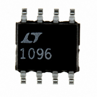
LTC1096CS8#PBF Linear Technology, LTC1096CS8#PBF Datasheet - Page 16

LTC1096CS8#PBF
Manufacturer Part Number
LTC1096CS8#PBF
Description
IC A/D CONV 8BIT SRL IN/OUT8SOIC
Manufacturer
Linear Technology
Datasheet
1.LTC1098CS8PBF.pdf
(32 pages)
Specifications of LTC1096CS8#PBF
Number Of Bits
8
Sampling Rate (per Second)
33k
Data Interface
Serial
Number Of Converters
1
Power Dissipation (max)
600µW
Voltage Supply Source
Single Supply
Operating Temperature
0°C ~ 70°C
Mounting Type
Surface Mount
Package / Case
8-SOIC (0.154", 3.90mm Width)
Number Of Elements
1
Resolution
8Bit
Architecture
SAR
Sample Rate
33KSPS
Input Polarity
Unipolar
Input Type
Voltage
Rated Input Volt
5V
Differential Input
Yes
Power Supply Requirement
Single
Single Supply Voltage (typ)
5V
Single Supply Voltage (min)
3V
Single Supply Voltage (max)
9V
Dual Supply Voltage (typ)
Not RequiredV
Dual Supply Voltage (min)
Not RequiredV
Dual Supply Voltage (max)
Not RequiredV
Power Dissipation
500mW
Differential Linearity Error
±1LSB(Typ)
Integral Nonlinearity Error
±1LSB
Operating Temp Range
0C to 70C
Operating Temperature Classification
Commercial
Mounting
Surface Mount
Pin Count
8
Package Type
SOIC N
Lead Free Status / RoHS Status
Lead free / RoHS Compliant
Available stocks
Company
Part Number
Manufacturer
Quantity
Price
LTC1096/LTC1096L
LTC1098/LTC1098L
APPLICATIONS INFORMATION
The wake-up time is inherently provided for the LTC1098(L)
with setup time = 1μs (see Figure 2).
Data Transfer
The CLK synchronizes the data transfer with each bit being
transmitted on the falling CLK edge and captured on the
rising CLK edge in both transmitting and receiving sys-
tems. The LTC1098(L) fi rst receives input data and then
transmits back the A/D conversion result (half duplex).
Because of the half duplex operation, D
be tied together allowing transmission over just three
wires: CS, CLK and DATA (D
Data transfer is initiated by a falling chip select (CS) signal.
After CS falls the LTC1098(L) looks for a start bit. After the
start bit is received, the 3-bit input word is shifted into the
D
conversion. After one null bit, the result of the conversion
16
IN
input which confi gures the LTC1098(L) and starts the
D
D
OUT
CLK
CLK
OUT
CS
CS
*AFTER COMPLETING THE DATA TRANSFER, IF FURTHER CLOCKS ARE APPLIED WITH CS LOW, THE ADC WILL OUTPUT ZEROS INDEFINITELY.
Hi-Z
HI-Z
t
WAKEUP
t
WAKEUP
t
t
suCS
suCS
IN
/D
OUT
).
NULL
BIT
NULL
BIT
(MSB)
(MSB)
IN
B7
B7
Figure 1. LTC1096(L) Operating Sequence
and D
B6
B6
t
CYC
OUT
t
B5
B5
CONV
t
CONV
may
B4
B4
B3
B3
t
CYC
B2
B2
ADDRESS IN
is output on the D
CS should be brought high. This resets the LTC1098(L) in
preparation for the next data exchange.
The LTC1096(L) does not require a confi guration input
word and has no D
feras shown in the LTC1096(L) operating sequence. After
CS falls, the fi rst CLK pulse enables D
bit, the A/D conversion result is output on the D
Bringing CS high resets the LTC1096(L) for the next data
exchange.
SHIFT MUX
B1
B1
CS
B0
B0
D
IN
B1
POWER
DOWN
1
1 NULL BIT
Hi-Z
B2
OUT
IN
D
B3
OUT
pin. A falling CS initiates data trans-
line. At the end of the data exchange
SHIFT A/D CONVERSION
RESULT OUT
1
B4
B5
B6
D
IN
B7*
2
OUT
POWER
DOWN
. After one null
Hi-Z
D
OUT
10968 F01
2
OUT
10968 AI01
10968fc
line.


