MCP3423-E/UN Microchip Technology, MCP3423-E/UN Datasheet - Page 6
MCP3423-E/UN
Manufacturer Part Number
MCP3423-E/UN
Description
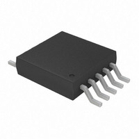
IC ADC 18BIT 3.75SPS 2CH 10-MSOP
Manufacturer
Microchip Technology
Specifications of MCP3423-E/UN
Data Interface
I²C, Serial
Number Of Bits
18
Sampling Rate (per Second)
3.75
Number Of Converters
1
Voltage Supply Source
Single Supply
Operating Temperature
-40°C ~ 125°C
Mounting Type
Surface Mount
Package / Case
10-TFSOP (0.118", 3.00mm Width)
Resolution (bits)
18bit
Sampling Rate
3.75SPS
Input Channel Type
Differential
Supply Voltage Range - Analog
2.7V To 5.5V
Supply Current
145µA
Lead Free Status / RoHS Status
Lead free / RoHS Compliant
For Use With
MCP3423EV - BOARD EVAL 18BIT 2CH ADC MCP3423
Lead Free Status / RoHS Status
Lead free / RoHS Compliant, Lead free / RoHS Compliant
Available stocks
Company
Part Number
Manufacturer
Quantity
Price

Part Number:
MCP3423-E/UN
Manufacturer:
MICROCHI
Quantity:
20 000


MCP3422/3/4
ELECTRICAL CHARACTERISTICS (CONTINUED)
DS22088C-page 6
Electrical Specifications: Unless otherwise specified, all parameters apply for T
CHn+ = CHn- = V
PGA Gain Error Match (Note 6)
Gain Error Drift (Note 6)
Offset Error
Offset Drift vs. Temperature
Common-Mode Rejection
Gain vs. V
Power Supply Rejection at DC
Input
Power Requirements
Voltage Range
Supply Current during
Conversion
Supply Current during Standby
Mode
I
High level input voltage
Low level input voltage
Low level output voltage
Hysteresis of Schmidt Trigger
for inputs (Note 7)
Supply Current when I
line is active
Input Leakage Current
Logic Status of I
Adr0 and Adr1 Pins
Adr0 and Adr1 Pins
Adr0 and Adr1 Pins
Pin Capacitance and I
Pin capacitance
I
Note 1:
2
2
C Digital Inputs and Digital Outputs
C Bus Capacitance
2:
3:
4:
5:
6:
7:
8:
9:
10: No voltage is applied at address pin (left “floating”).
Parameters
DD
Any input voltage below or greater than this voltage causes leakage current through the ESD diodes at the input pins.
This parameter is ensured by characterization and not 100% tested.
This input impedance is due to 3.2 pF internal input sampling capacitor.
This parameter is ensured by design and not 100% tested.
The total conversion speed includes auto-calibration of offset and gain.
INL is the difference between the endpoints line and the measured code at the center of the quantization band.
Includes all errors from on-board PGA and V
This parameter is ensured by characterization and not 100% tested.
MCP3423 and MCP3424 only.
Addr_Float voltage is applied at address pin.
2
REF
C Address Pins (Note 8)
/2, V
2
2
C bus
C Bus Capacitance
INCOM
= V
Addr_Float
Addr_High
Addr_Low
REF
V
Sym
I
I
I
C
V
V
V
V
HYST
I
DDA
DDS
V
DDB
I
C
ILH
ILL
PIN
OS
DD
OL
IH
IL
b
/2. All ppm units use 2*V
0.05V
0.75V
0.35V
0.7V
V
Min
2.7
—
—
—
—
—
—
—
—
—
—
—
—
—
—
—
-1
—
—
—
SS
DD
DD
DD
DD
REF
.
V
105
100
145
135
110
Typ
0.1
0.3
DD
15
15
50
—
—
—
—
—
—
—
—
—
—
—
—
5
4
REF
/2
as differential full scale range.
0.3V
0.2V
0.6V
V
V
Max
180
400
5.5
0.4
55
10
10
—
—
—
—
—
—
—
—
—
—
—
1
1
DD
DD
DD
DD
DD
A
= -40°C to +85°C, V
ppm/°C
ppm/V
nV/°C
Units
µV
dB
dB
dB
µA
µA
µA
µA
µA
µA
pF
pF
%
V
V
V
V
V
V
V
V
© 2009 Microchip Technology Inc.
Between any 2 PGA settings
PGA=1, DR=3.75 SPS
Tested at PGA = 1
DR = 3.75 SPS
at DC and PGA =1,
at DC and PGA =8, T
T
PGA = 1
T
PGA = 1
V
V
V
at SDA and SCL pins
at SDA and SCL pins
I
f
Device is in standby mode while
I
V
V
The device reads logic low.
The device reads logic high.
Read pin voltage if voltage is
applied to the address pin.
(Note 9)
Device outputs float output
voltage (V
pin, if left “floating”. (Note 10)
OL
SCL
2
A
A
DD
DD
DD
IH
IL
C bus is active
= +25°C, V
= +25°C, V
= 3 mA
= GND
= 5.5V
DD
= 5.0V
= 3.0V
= 5.0V
= 100 kHz
= +5.0V, V
DD
/2) on the address
DD
DD
Conditions
= 2.7V to 5.5V,
= 2.7V to 5.5V,
SS
= 0V,
A
= +25°C
Related parts for MCP3423-E/UN
Image
Part Number
Description
Manufacturer
Datasheet
Request
R

Part Number:
Description:
IC ADC 18BIT 3.75SPS 2CH 10-DFN
Manufacturer:
Microchip Technology
Datasheet:

Part Number:
Description:
Manufacturer:
Microchip Technology Inc.
Datasheet:
Part Number:
Description:
Manufacturer:
Microchip Technology Inc.
Datasheet:
Part Number:
Description:
Manufacturer:
Microchip Technology Inc.
Datasheet:
Part Number:
Description:
Manufacturer:
Microchip Technology Inc.
Datasheet:
Part Number:
Description:
Manufacturer:
Microchip Technology Inc.
Datasheet:
Part Number:
Description:
Manufacturer:
Microchip Technology Inc.
Datasheet:
Part Number:
Description:
Manufacturer:
Microchip Technology Inc.
Datasheet:
Part Number:
Description:
Manufacturer:
Microchip Technology Inc.
Datasheet: